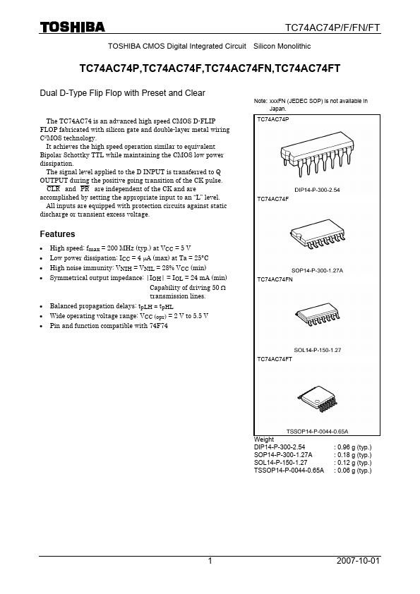
TC74AC74FN
TC74AC74FN is DUAL D TYPE FLIP FLOP WITH PRESET AND CLEAR manufactured by Toshiba.
- Part of the TC74AC74F comparator family.
- Part of the TC74AC74F comparator family.
TC74AC74P/F/FN/FT
TOSHIBA CMOS Digital Integrated Circuit Silicon Monolithic
TC74AC74P,TC74AC74F,TC74AC74FN,TC74AC74FT
Dual D-Type Flip Flop with Preset and Clear
The TC74AC74 is an advanced high speed CMOS D-FLIP FLOP fabricated with silicon gate and double-layer metal wiring C2MOS technology.
It achieves the high speed operation similar to equivalent Bipolar Schottky TTL while maintaining the CMOS low power dissipation.
The signal level applied to the D INPUT is transferred to Q OUTPUT during the positive going transition of the CK pulse.
CLR and PR are independent of the CK and are acplished by setting the appropriate input to an “L” level.
All inputs are equipped with protection...