Datasheet4U Logo Datasheet4U.com

TC74ACT573FW - OCTAL D-TYPE LATCH WITH 3-STATE OUTPUT

Download the TC74ACT573FW datasheet PDF. This datasheet also covers the TC74ACT573F variant, as both devices belong to the same octal d-type latch with 3-state output family and are provided as variant models within a single manufacturer datasheet.

Key Features

  • High speed: tpd = 5.5 ns (typ. ) at VCC = 5 V.
  • Low power dissipation: ICC = 8 µA (max) at Ta = 25°C.
  • Compatible with TTL outputs: VIL = 0.8 V (max) VIH = 2.0 V (min).
  • Symmetrical output impedance: |IOH| = IOL = 24 mA (min) Capability of driving 50 Ω transmission lines.
  • Balanced propagation delays: tpLH ∼.
  • tpHL.
  • Pin and function compatible with 74F573 Note: xxxFW (JEDEC SOP) is not available in Japan. TC74ACT573P TC74ACT573F TC74ACT5.

📥 Download Datasheet

Note: The manufacturer provides a single datasheet file (TC74ACT573F_ToshibaSemiconductor.pdf) that lists specifications for multiple related part numbers.

Datasheet Details

Part number TC74ACT573FW
Manufacturer Toshiba
File Size 211.12 KB
Description OCTAL D-TYPE LATCH WITH 3-STATE OUTPUT
Datasheet download datasheet TC74ACT573FW Datasheet

Full PDF Text Transcription (Reference)

The following content is an automatically extracted verbatim text from the original manufacturer datasheet and is provided for reference purposes only.

View original datasheet text
TC74ACT573P/F/FW/FT TOSHIBA CMOS Digital Integrated Circuit Silicon Monolithic 
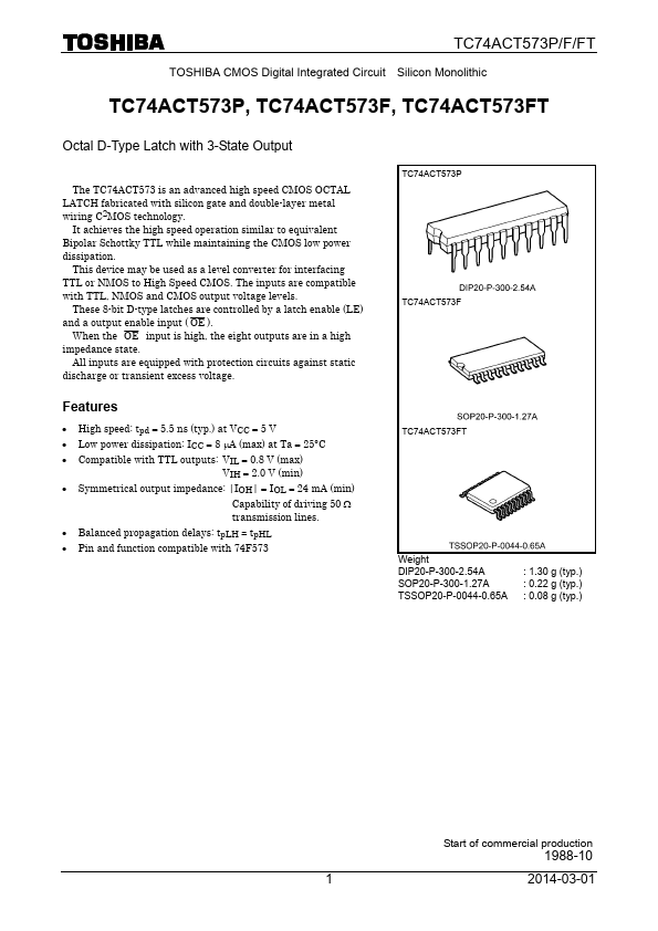
TC74ACT573P,TC74ACT573F,TC74ACT573FW,TC74ACT573FT Octal D-Type Latch with 3-State Output The TC74ACT573 is an advanced high speed CMOS OCTAL LATCH fabricated with silicon gate and double-layer metal wiring C2MOS technology. It achieves the high speed operation similar to equivalent Bipolar Schottky TTL while maintaining the CMOS low power dissipation. This device may be used as a level converter for interfacing TTL or NMOS to High Speed CMOS. The inputs are compatible with TTL, NMOS and CMOS output voltage levels. 
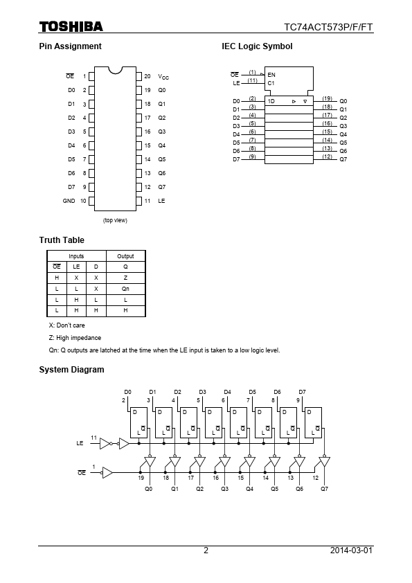
These 8-bit D-type latches are controlled by a latch enable (LE) and a output enable input ( OE ). When the OE input is high, the eight outputs are in a high impedance state.