TC74HC4052AF
TC74HC4052AF is 8-CHANNEL ANALOG MULTIPLEXER/DEMULITIPLEXER manufactured by Toshiba.
- Part of the TC74HC4051 comparator family.
- Part of the TC74HC4051 comparator family.
TC74HC4051,4052,4053AP/AF/AFT
TOSHIBA CMOS Digital Integrated Circuit Silicon Monolithic
TC74HC4051AP, TC74HC4051AF, TC74HC4051AFT TC74HC4052AP, TC74HC4052AF, TC74HC4052AFT TC74HC4053AP, TC74HC4053AF, TC74HC4053AFT
TC74HC4051AP/AF/AFT
8-Channel Analog
Multiplexer/Demultiplexer
TC74HC4052AP/AF/AFT
Dual 4-Channel Analog Multiplexer/Demultiplexer
TC74HC4053AP/AF/AFT
Triple 2-Channel Analog Multiplexer/Demultiplexer
The TC74HC4051A/4052A/4053A are high speed CMOS ANALOG MULTIPLEXER/DEMULTIPLEXER fabricated with silicon gate C2MOS technology. They achieve the high speed operation similar to equivalent LSTTL while maintaining the CMOS low power dissipation.
The TC74HC4051A has an 8 channel configuration, the TC74HC4052A has a 4 channel × 2 configuration and the TC74HC4053A has a 2 channel × 3 configuration.
The digital signal to the control terminal turns “ON” the corresponding switch of each channel a large amplitude signal (VCC
- VEE) can then be switched by the small logical amplitude (VCC
- GND) control signal.
For example, in the case of VCC = 5 V, GND = 0 V, VEE =
- 5 V, signals between
- 5 V and +5 V can be switched from the logical circuit with a single power supply of 5 V. As the ON-resistance of each switch is low, they can be connected to circuits with low input impedance.
All inputs are equipped with protection circuits against static discharge or transient excess voltage.
Features
- High speed: tpd = 15 ns (typ.) at VCC = 5 V, VEE = 0 V
- Low power dissipation: ICC = 4 μA (max) at Ta = 25°C
- High noise immunity: VNIH = VNIL = 28% VCC (min)
- Low ON resistance: RON = 50 Ω (typ.) at VCC
- VEE = 9 V
- High noise immunity: THD = 0.02% (typ.) at VCC
- VEE = 9 V
- Pin and function patible with 4051/4052/4053B
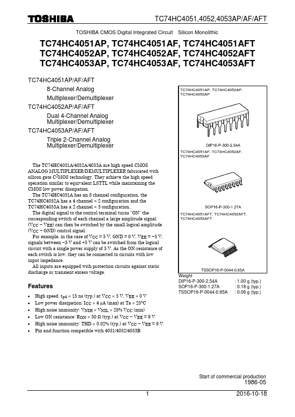
TC74HC4051AP, TC74HC4052AP, TC74HC4053AP
TC74HC4051AF, TC74HC4052AF,...