Datasheet4U Logo Datasheet4U.com

TC7MBL3253CFT - Dual 1-of-4 FET Multiplexer/Demultiplexer

Download the TC7MBL3253CFT datasheet PDF. This datasheet also covers the TC7MBL3253CFK variant, as both devices belong to the same dual 1-of-4 fet multiplexer/demultiplexer family and are provided as variant models within a single manufacturer datasheet.

General Description

2.

The TC7MBL3253CFT is a low-voltage/low-capacitance CMOS dual 1-of-4 Multiplexer/Demultiplexer.

The low on-resistance of the switch allows connections to be made with minimal propagation delay time.

Key Features

  • (1) Wide operating temperature range: Topr = -40 to 125  (Note 1) (2) Operating voltage: VCC = 1.65 to 3.6 V (3) ON capacitance: CI/O = 13 pF Switch On (typ. ) @VCC = 3.0 V (4) ON resistance: RON = 9 Ω (typ. ) @VCC = 3.0 V, VI/O = 0 V (5) ESD performance: MM ≥ ±200 V, HBM ≥ ±2000 V (6) Power-down protection for inputs (OE, S1, S0 and I/O) (7) Package: TSSOP16 Note 1: Operating Range spec of Topr = -40  to 125  is applicable only for the products which manufactured after April 2020. 4. Packaging.

📥 Download Datasheet

Note: The manufacturer provides a single datasheet file (TC7MBL3253CFK_ToshibaSemiconductor.pdf) that lists specifications for multiple related part numbers.

Datasheet Details

Part number TC7MBL3253CFT
Manufacturer Toshiba
File Size 381.07 KB
Description Dual 1-of-4 FET Multiplexer/Demultiplexer
Datasheet download datasheet TC7MBL3253CFT Datasheet

Full PDF Text Transcription (Reference)

The following content is an automatically extracted verbatim text from the original manufacturer datasheet and is provided for reference purposes only.

View original datasheet text
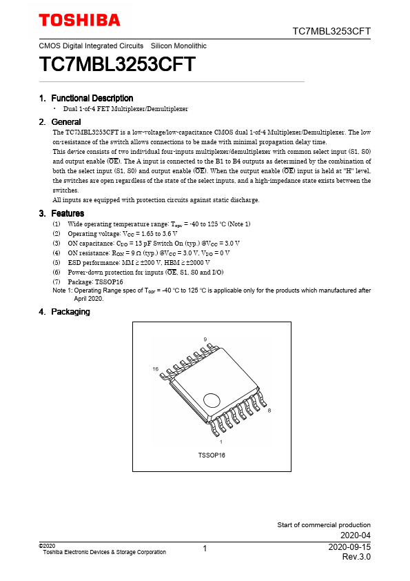
CMOS Digital Integrated Circuits Silicon Monolithic TC7MBL3253CFT TC7MBL3253CFT 1. Functional Description • Dual 1-of-4 FET Multiplexer/Demultiplexer 2. General The TC7MBL3253CFT is a low-voltage/low-capacitance CMOS dual 1-of-4 Multiplexer/Demultiplexer. The low on-resistance of the switch allows connections to be made with minimal propagation delay time. This device consists of two individual four-inputs multiplexer/demultiplexer with common select input (S1, S0) and output enable (OE). The A input is connected to the B1 to B4 outputs as determined by the combination of both the select input (S1, S0) and output enable (OE).