TC7SP98TU Description
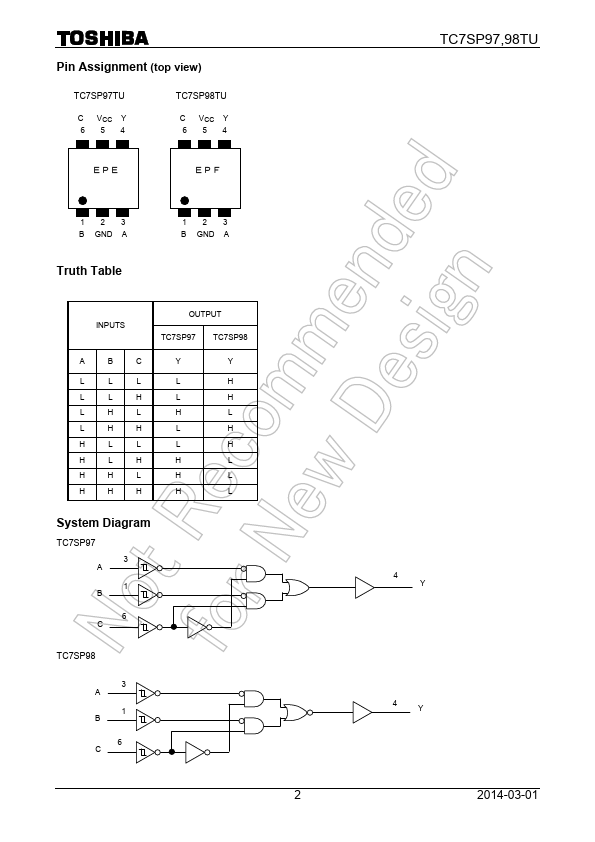
Designed for use in 1.5 V, 1.8 V, 2.5 V or 3.3 V systems, it achieves high speed operation while maintaining the CMOS low power dissipation. It is also designed with over voltage tolerant inputs and outputs up to 3.6 V. It independently consists of three circuits for Multiple Function Gate.
TC7SP98TU Key Features
- Low-voltage operation : VCC = 1.2 to 3.6 V
- High-speed operation
- Output current
- Latch-up performance : -300 mA
- ESD performance
- Package
- Power-down protection is provided on all inputs and outputs