TC7WPB306FK Overview
Key Specifications
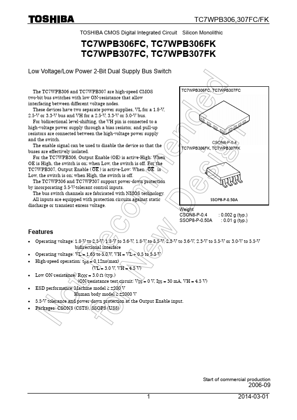
Package: VSSOP
Mount Type: Surface Mount
Pins: 8
Operating Voltage: 2.5 V
Key Features
- Operating voltage: 1.8-V to 2.5-V, 1.8-V to 3.6-V, 1.8-V to 5.5-V, 2.3-V to 3.6-V, 2.3-V to 5.5-V or 3.0-V to 5.5-V bidirectional interface
- Operating voltage: VL = 1.65 to 5.0 V, VH = VL + 0.5 to 5.5 V
- High-speed operation: tpd = 0.12ns(max) (VL = 3.0 V, VH = 4.5 V)
- Low ON-resistance: RON = 3.0 Ω (typ.) (ON-resistance test circuit: VIS = 0 V, IIS = 30 mA, VH = 4.5 V)
- ESD performance: Machine model ≥ ±200 V Human body model ≥ ±2000 V