TC7WPN3125FK
Key Features
- Output current : IOH / IOL = ±3 mA (min) (VCC = 3.0 V) IOH / IOL = ±2mA (min) (VCC = 2.3 V) IOH / IOL = ±0.5 mA (min) (VCC = 1.65 V)
- Latch-up performance: -300 mA
- ESD performance: Machine model ≥ ±200 V Human body model ≥ ±2000 V
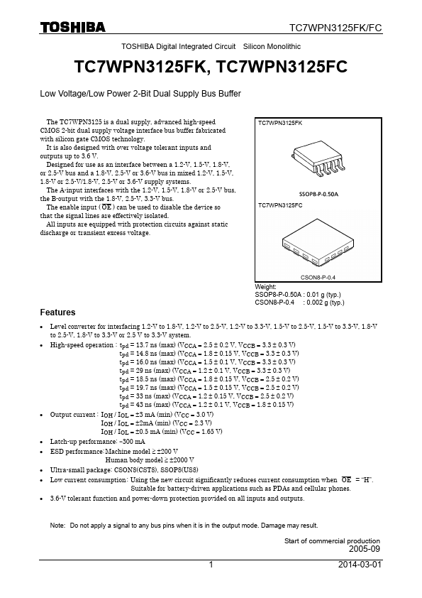
- Ultra-small package: CSON8(CST8), SSOP8(US8)
- 3.6-V tolerant function and power-down protection provided on all inputs and outputs