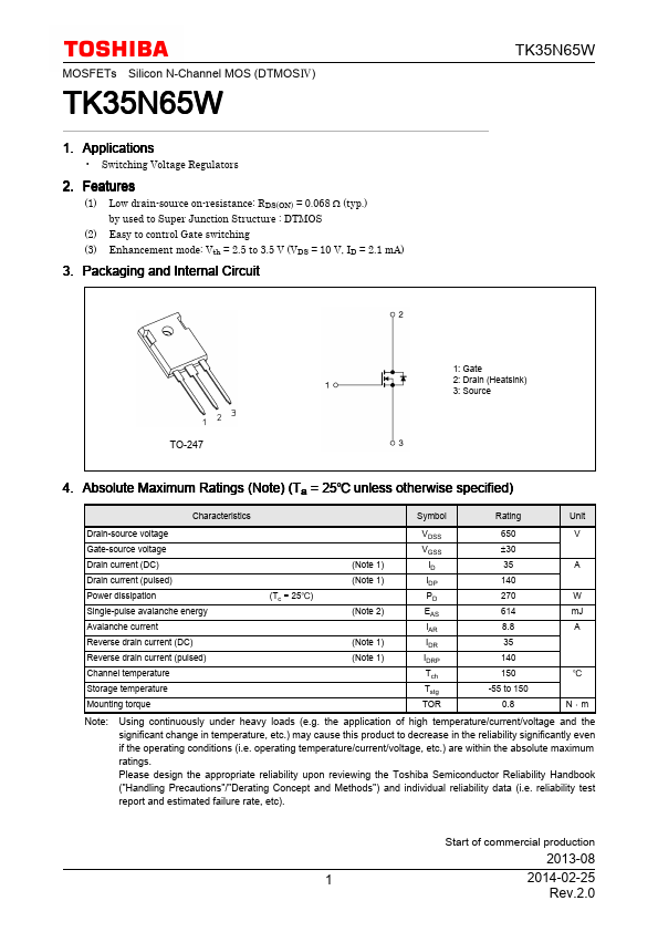
(1) (2) (3) Low drain-source on-resistance: RDS(ON) = 0.068 Ω (typ. ) by used to Super Junction Structure : DTMOS Easy to control Gate switching Enhancement mode: Vth = 2.5 to 3.5 V (VDS = 10 V, ID = 2.1 mA)
3. Packaging and Internal Circuit
1: Gate 2: Drain (Heatsink) 3: Source
TO-247
4. Absolute Maximum Ratings (Note) (Ta = 25 unless otherwise specified)
Characteristics Drain-source voltage Gate-source voltage Drain current (DC) Drain current (pulsed) Power dissipation Single-pulse avalanc.
Full PDF Text Transcription for TK35N65W (Reference)
Note: Below is a high-fidelity text extraction (approx. 800 characters) for
TK35N65W. For precise diagrams, and layout, please refer to the original PDF.
TK35N65W MOSFETs Silicon N-Channel MOS (DTMOS) TK35N65W 1. Applications • Switching Voltage Regulators 2. Features (1) (2) (3) Low drain-source on-resistance: RDS(ON) = ...
View more extracted text
ors 2. Features (1) (2) (3) Low drain-source on-resistance: RDS(ON) = 0.068 Ω (typ.) by used to Super Junction Structure : DTMOS Easy to control Gate switching Enhancement mode: Vth = 2.5 to 3.5 V (VDS = 10 V, ID = 2.1 mA) 3. Packaging and Internal Circuit 1: Gate 2: Drain (Heatsink) 3: Source TO-247 4.