The following content is an automatically extracted verbatim text
from the original manufacturer datasheet and is provided for reference purposes only.
View original datasheet text
TK40J60T
TOSHIBA Field Effect Transistor Silicon N Channel MOS Type (DTMOS)
www.DataSheet4U.com
TK40J60T
Switching Regulator Applications
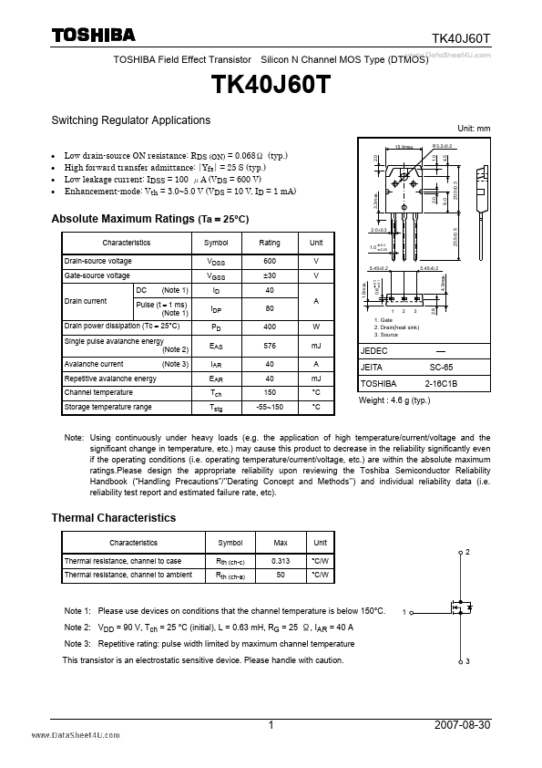
15.9max. Ф3.2±0.2 1.0 4.5 9.0
Unit: mm
3.3max.
Absolute Maximum Ratings (Ta = 25°C)
Characteristics Drain-source voltage Gate-source voltage DC Drain current (Note 1) Symbol VDSS VGSS ID IDP PD EAS IAR EAR Tch Tstg Rating 600 ±30 40 80 400 576 40 40 150 -55~150 A W mJ A mJ °C °C Unit V V
1.8max. 0.6-0.1
+0.3
1.0 -0.25
+0.3
5.45±0.2
5.45±0.2 4.8max. 1 2 3 2.8
Pulse (t = 1 ms) (Note 1)
Drain power dissipation (Tc = 25°C) Single pulse avalanche energy (Note 2) Avalanche current Repetitive avalanche energy Channel temperature Storage temperature range (Note 3)
1. Gate 2. Drain(heat sink) 3. Source
JEDEC JEITA TOSHIBA
⎯ SC-65 2-16C1B
Weight : 4.