TK45P03M1
Features
(1) (2) (3) (4) (5) High-speed switching Low gate charge: QSW = 8.0 n C (typ.) Low drain-source on-resistance: RDS(ON) = 6.5 mΩ (typ.) (VGS = 10 V) Low leakage current: IDSS = 10 µA (max) (VDS = 30 V) Enhancement mode: Vth = 1.3 to 2.3 V (VDS = 10 V, ID = 0.2 m A)
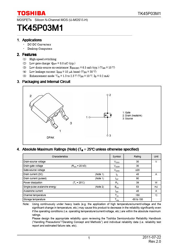
3. Packaging and Internal Circuit
1: Gate 2: Drain (heatsink) 3: Source
DPAK
4. Absolute Maximum Ratings (Note) (Ta = 25 unless otherwise specified)
Characteristics Drain-source voltage Drain-gate voltage Gate-source voltage Drain current (DC) Drain current (pulsed) Power dissipation Single-pulse avalanche energy Avalanche current Channel temperature Storage temperature (Tc = 25) (Note 2) (Note 1) (Note 1) (RGS = 20 kΩ) Symbol VDSS VDGR VGSS ID IDP PD EAS IAR Tch Tstg Rating 30 30 ±20 45 90 39 53 45 150 -55 to 150 W m J A A Unit V
Note:
Using continuously under heavy loads (e.g. the application of high temperature/current/voltage and the significant change in temperature, etc.) may cause this product to...