Toshiba 2SJ511
Silicon P-Channel MOSFET
| Part No. | 2SJ511 |
|---|---|
| Datasheet | 2SJ511 Download |
| Manufacturer |  Toshiba |
| Description | Silicon P-Channel MOSFET |
| Buy | Stock & Price |
APPLICATIONS
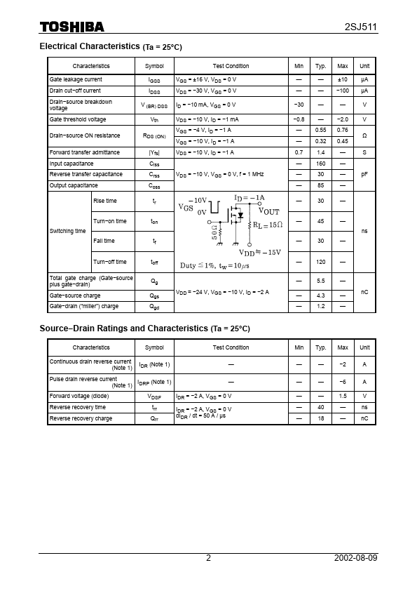
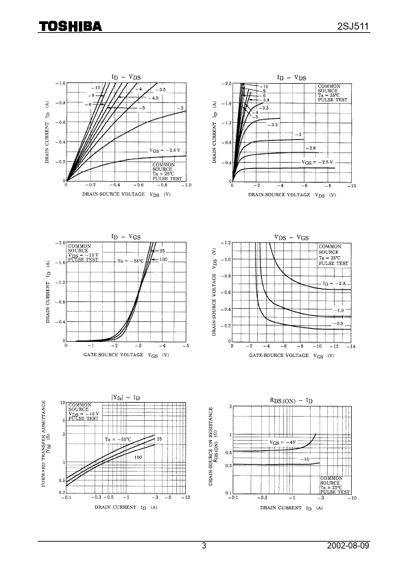
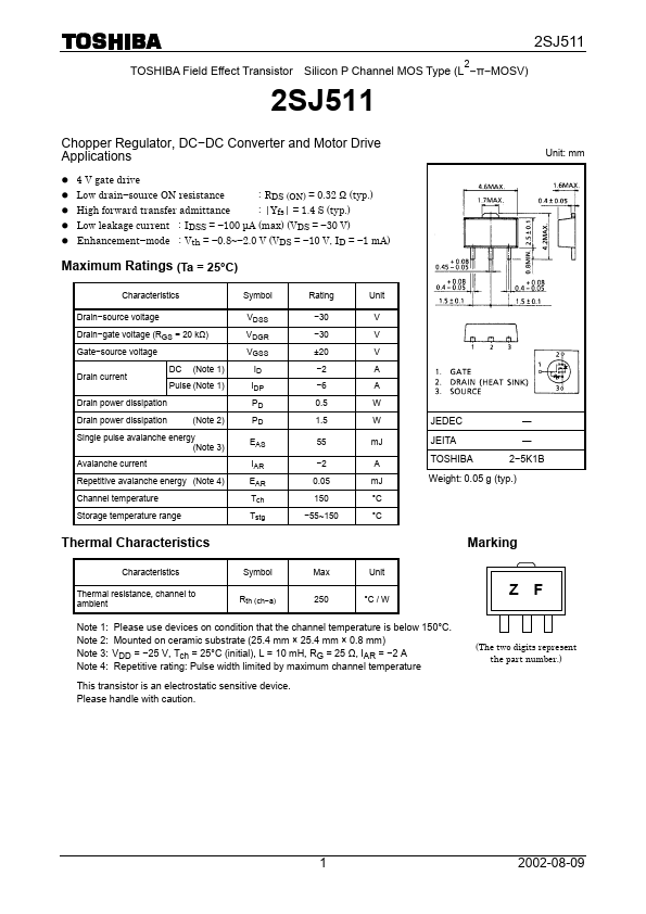
l 4 V gate drive l Low drain−source ON resistance : RDS (ON) = 0.32 Ω (typ.) l High forward transfer admittance : |Yfs| = 1.4 S (typ.) l Low leakage current : IDSS = −100 µA (max) (VDS = −30 V) l Enhancement−mode : Vth = −0.8~−2.0 V (VDS = −10 V, ID = −1 mA)MAXIMUM RATINGS
(Ta = 25°C) Unit: mm Characteristics Drain−source voltage Drain−gate voltage (RGS = 20 kΩ) Gate−source voltage Drain current DC (Note 1) Pulse (Note 1) Drain power dissipation Drain power dissipation (Note 2) Single pulse avalanche energy (Note 3) Avalanche current Repetitive avalanche energy (Note 4) Channel temperature Storage temperature range Thermal Characteristics Symbol VDSS VDGR VGSS ID IDP PD PD EAS IAR EAR Tch Tstg Rating −30 −30 ±20 −2 −6 0.5 1.5 55 −2 0.05 150 −55~150 Unit V V V A A W W mJ A mJ °C °C JEDEC ― JEITA ― TOSHIBA 2−5K1B Weight: 0.05 g (typ.) Marking Characteristics Symbol Max Unit Thermal resistance, channel to ambient Rth (ch−a) 250 °C / W Note 1: Please use devices on condition that the channel temperature is below 150°C.