Datasheet4U Logo Datasheet4U.com

74HC4049D - Hex Buffer

General Description

2.

The 74HC4049D and 74HC4050D are high speed CMOS HEX BUFFERs fabricated with silicon gate C2MOS technology.

Key Features

  • (1) Wide operating temperature range: Topr = -40 to 125.
  • (Note 1) (2) High speed: tpd = 8 ns (typ. ) at VCC = 6.0 V (3) Low power dissipation: ICC = 1.0 µA (max) at Ta = 25.
  • (4) Balanced propagation delays: tPLH ≈ tPHL (5) Wide operating voltage range: VCC(opr) = 2.0 V to 6.0 V Note 1: Operating Range spec of Topr = -40.
  • to 125.
  • is applicable only for the products which manufactured after July 2020. 4. 
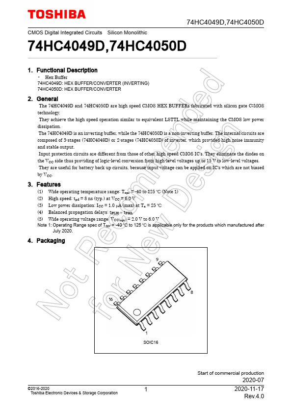
Packaging SOIC16 ©2016-2020 1 Toshiba Electronic Devices & Storage Corp.

📥 Download Datasheet

Full PDF Text Transcription (Reference)

The following content is an automatically extracted verbatim text from the original manufacturer datasheet and is provided for reference purposes only.

View original datasheet text
74HC4049D,74HC4050D CMOS Digital Integrated Circuits Silicon Monolithic 74HC4049D,74HC4050D 1. Functional Description • Hex Buffer 74HC4049D: HEX BUFFER/CONVERTER (INVERTING) 74HC4050D: HEX BUFFER/CONVERTER 2. General The 74HC4049D and 74HC4050D are high speed CMOS HEX BUFFERs fabricated with silicon gate C2MOS technology. They achieve the high speed operation similar to equivalent LSTTL while maintaining the CMOS low power dissipation. The 74HC4049D is an inverting buffer, while the 74HC4050D is a non-inverting buffer. The internal circuits are composed of 3-stages (74HC4049D) or 2-stages (74HC4050D) of inverter, which provided high noise immunity and stable output. Input protection circuits are different from those of other high speed CMOS IC's.