TA2025P
Feature
- High voltage gain : GVO = 100d B (typ.) (VCC = 9V, f = 1k Hz)
- No input coupling capacitor
- Low noise (equivalent noise voltage)
: VNI = 0.6µVrms (typ.) (VCC = 9V, Rg = 620Ω、 BW = 20Hz~20k Hz, NAB EQ)
- Low distortion: THD = 0.01% (typ.)
- Operating supply voltage range: VCC (opr.) = 6~16V
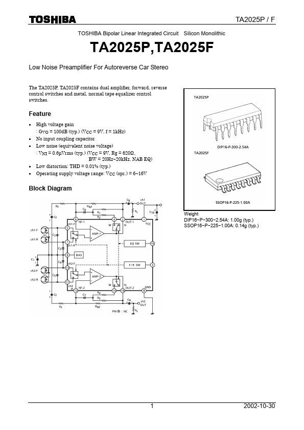
Block Diagram
Weight DIP16- P- 300- 2.54A: 1.00g (typ.) SSOP16- P- 225- 1.00A: 0.14g (typ.)
1 2002-10-30
Application Information
1. Forward, reverse select switch (1) Threshold voltage Pin(3) is coupled to the base of Q1 (PNP-Tr) as shown in Fig.1. Threshold voltage (pin(3)) = 0.7V
Reverse Forward
0~0.5V 1.0~VCC
(2) The remended forward, reverse select circuit is shown in Fig.2.
TA2025P / F
(3) I3 (in Fig.1) I3 = 12µA (max., Ta = 25°C)
2. Equalizer control switch Pin(15) is coupled to the base of Q2 (PNP-Tr) as shown in Fig.3. The emitter potential of Q2 is 3.9V (DC). Threshold voltage (pin(15)) = 2.8V
Metal Normal
3.2~16V 0~2.4V
3. C2 / C3 / C4 / C5 Capacitor C2~C5 may be required for...