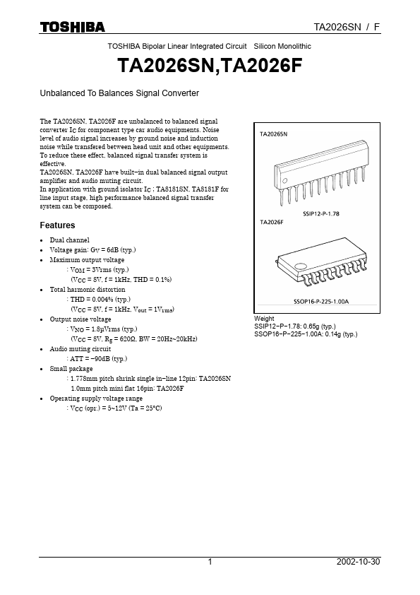
TA2026F
Features
- Dual channel
- Voltage gain: GV = 6d B (typ.)
- Maximum output voltage
: VOM = 3Vrms (typ.) (VCC = 8V, f = 1k Hz, THD = 0.1%)
- Total harmonic distortion : THD = 0.004% (typ.) (VCC = 8V, f = 1k Hz, Vout = 1Vrms)
- Output noise voltage : VNO = 1.8µVrms (typ.) (VCC = 8V, Rg = 620Ω, BW = 20Hz~20k Hz)
- Audio muting circuit : ATT =
- 90d B (typ.)
- Small package : 1.778mm pitch shrink single in- line 12pin: TA2026SN 1.0mm pitch mini flat 16pin: TA2026F
- Operating supply voltage range : VCC (opr.) = 5~12V (Ta = 25°C)
Weight SSIP12- P- 1.78: 0.65g (typ.) SSOP16- P- 225- 1.00A: 0.14g (typ.)
1 2002-10-30
Block Diagram
TA2026SN / F
2 2002-10-30
Maximum Ratings (Ta = 25°C)
TA2026SN / F
Characteristic
Symbol
Rating
Unit
Supply voltage
Power dissipation
TA2026SN TA2026F
Operating temperature
Storage temperature
VCC PD (Note)
Topr Tstg
15 750 350 -30~85 -55~150
V m W
°C °C
(Note) Derated above Ta = 25°C in the proportion of 6m W / °C for TA2026SN, 2.8m W / °C for TA2026F.
Electric...