TA2092AN
Features
- -
- -
- - 4 channel BTL linear drivers Fixed voltage gain: GV = 15.5d B (typ.) High output power Thermal shutdown circuit Input reference voltage short protection Operating voltage range: VCC (opr) = 4.5~10.0 V (Ta = 25°C) Weight: 1.2 g (typ.)
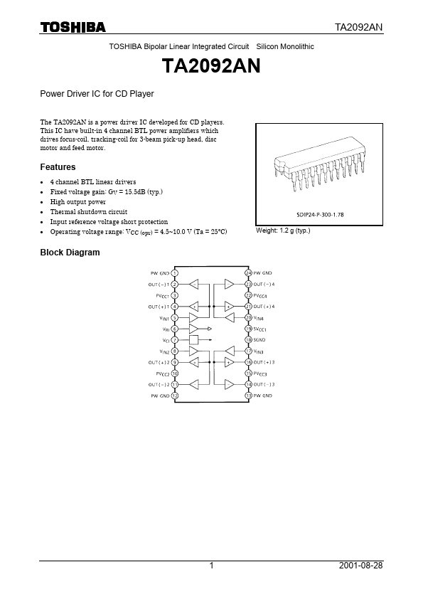
Block Diagram
2001-08-28
Terminal Explanation
Terminal No. 1 Symbol Function Equivalent Circuit
Power GND PW GND
- Connected to substrate.
- pin 1, 12, 13, 24 are connected inside. OUT (- ) 1 Inverted output for CH1 Supply terminal of output stage for CH1
- Supply terminal of output stage are not connected to other channel terminal.
PVCC1
OUT (+) 1 Non-inverted output for CH1
VIN1
Input for CH1
- Not biased inside
Input reference voltage
- Under condition of VRI ≤ 1.1 V, internal bias circuit is shut off.
- No signal input condition: VRI = VIN
Output reference voltage
- VOUT = VCI = (VCC- VF) /2
8 9 10 11 12 13 14 15 16 17 18 19 20 21 22 23 24
VIN2
Input for CH2
OUT (+) 2 Non-inverted...