TA8030F
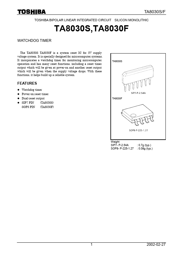
FEATURES l Watchdog timer l Power-on reset timer l Dual-reset output l SIP7 PIN (TA8030S)
SOP8 PIN (TA8030F)
TA8030S TA8030F
Weight
SIP7- P-2.54A
: 0.7g (typ.)
SOP8- P-225-1.27 : 0.08g (typ.)
1 2002-02-27
BLOCK DIAGRAM AND PIN LAYOUT
TA8030S/F
Note:The TA8030S and TA8030F are the same chip; only the packages are different.
2 2002-02-27
TA8030S/F
PIN DESCRIPTION
PIN No. TA80305 TA8030F
44 56 67 78 ―5
SYMBOL
DESCRIPTION
WD TC
RST1 GND ADJ VCC RST2 NC
Clock input pin for watchdog timer. If this IC is only used as a power-on reset timer, this pin is connected to RST1 .
Time setting pin for the reset and watchdog timers. R1 leads to VCC, and C1 leads to GND.
Supplies an NPN transistor open-collector output.
- Generates a reset signal determined by the CR bination connected to the TC pin.
- Supplies reset pulses intermittently if no clock is given to the WD pin.
Grounded
VCC detect voltage (1) adjusting pin. The detection voltage is 4.6V when this pin is grounded ;...