TB62D612FTG
TB62D612FTG is manufactured by Toshiba.
TOSHIBA BiCD Process Integrated Circuit Silicon Monolithic
24-Channel Constant-Current LED Driver of the 3.3-V or 5-V Power Supply Voltage Operation
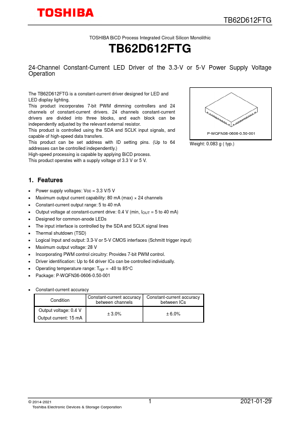
The TB62D612FTG is a constant-current driver designed for LED and LED display lighting. This product incorporates 7-bit PWM dimming controllers and 24 channels of constant-current drivers. 24 channels constant-current drivers are divided into three blocks, and each block can be independently adjusted by the relevant external resistor. This product is controlled using the SDA and SCLK input signals, and capable of high-speed data transfers. This product can be set address with ID setting pins. (Up to 64 addresses can be...


