TB9032FNG
TB9032FNG is Automotive CXPI communication driver receiver manufactured by Toshiba.
Preliminary
CDMOS Linear Integrated Circuits Silicon Monolithic
Automotive CXPI munication driver receiver IC
1. INTRODUCTION
TB9032FNG is a driver receiver IC that is pliant with ISO 20794-4 for the CXPI (Clock Extension Peripheral Interface) munication. It can switch between mander and responder nodes using the external pin. When in Sleep Mode, it enters a standby state with low power consumption. In addition, it is equipped with fault detection functions including overheat detection and low voltage detection, and stops output when an abnormality is detected.
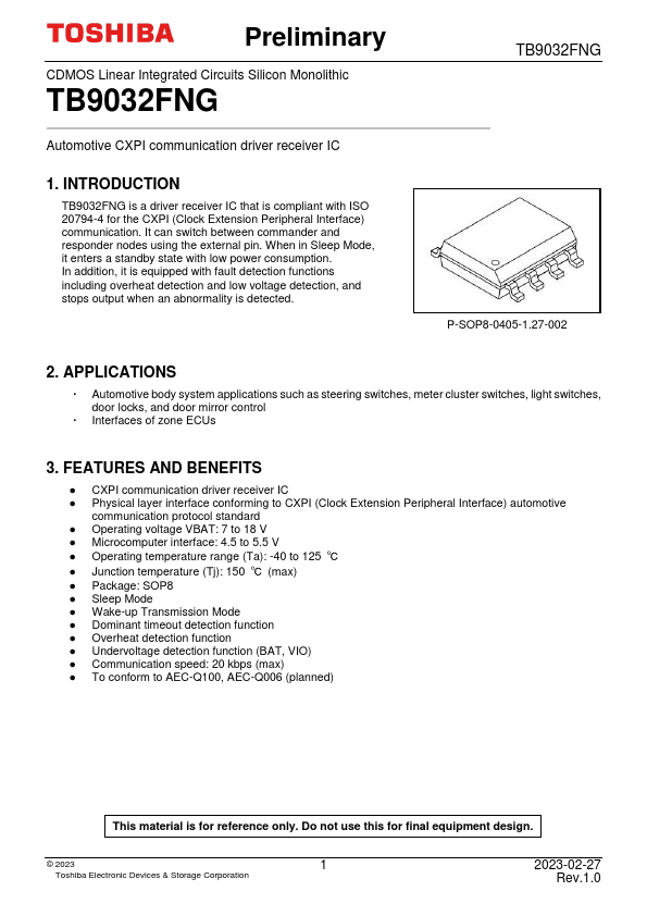
P-SOP8-0405-1.27-002
2. APPLICATIONS
- Automotive body system applications such as steering...


