TC74AC174FN
TC74AC174FN is Hex D-Type Flip Flop with Clear manufactured by Toshiba.
Features
- High speed: fmax = 180 MHz (typ.) at VCC = 5 V
- Low power dissipation: ICC = 8 µA (max) at Ta = 25°C
- High noise immunity: VNIH = VNIL = 28% VCC (min)
- Symmetrical output impedance: |IOH| = IOL = 24 m A (min)
Capability of driving 50 Ω transmiss Dionatlain Sehs.eet4U.
- Balanced propagation delays: tp LH ∼- tp HL
- Wide operating voltage range: VCC (opr) = 2 to 5.5 V
- Pin and function patible with 74F174
Data Shee
.
Data Sheet4 U .
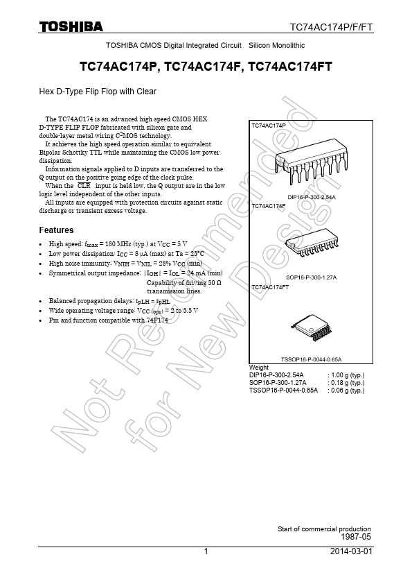
Weight DIP16-P-300-2.54A SOP16-P-300-1.27A SOP16-P-300-1.27 SOL16-P-150-1.27 TSSOP16-P-0044-0.65A
: 1.00 g (typ.) : 0.18 g (typ.) : 0.18 g (typ.) : 0.13 g (typ.) : 0.06 g (typ.)
TC74AC174FT
2006-02-01
..
Pin Assignment
TC74AC174P/F/FN/FT
IEC Logic Symbol et4U.
CLR 1 Q1 2 D1 3 D2 4 Q2 5 D3 6 Q3 7
GND 8
(top view)
16 VCC 15 Q6 14 D6 13 D5 12 Q5 11 D4 10 Q4 9 CK
CLR (1) R
CK (9)
C1
D1 (3) D2 (4) D3 (6) D4 (11) D5 (13) D6 (14)
1D
Truth Table
Inputs CLR D
LX HL HH HX
CK X
X: Don’t care
Output Q L L H Qn
Function
Clear ― ―
No...