- Part: TC74AC273FW
- Description: OCTAL D TYPE FLIP FLOP WITH CLEAR
- Manufacturer: Toshiba
- Size: 205.69 KB
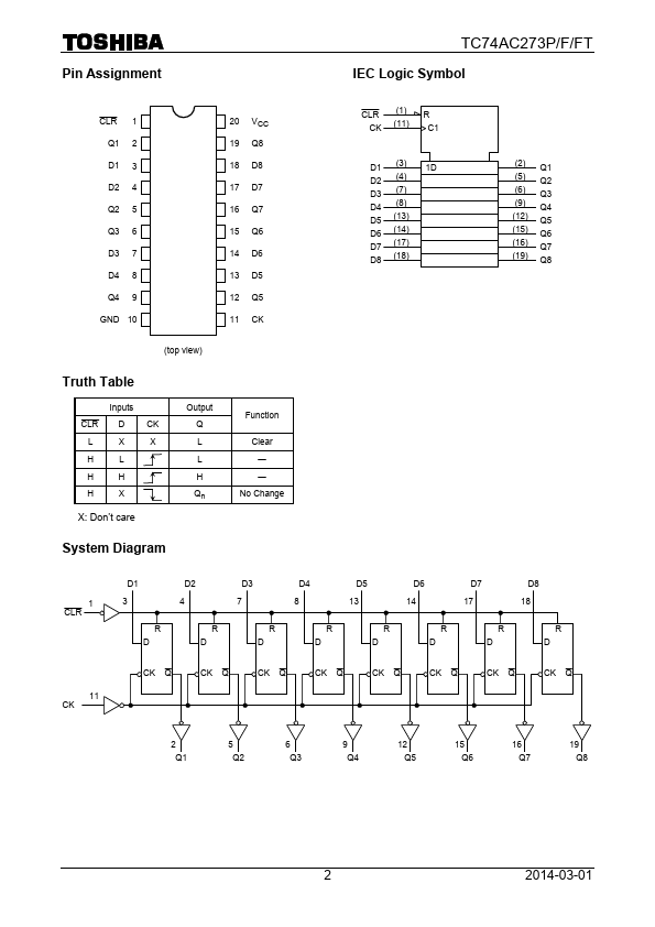 Page 2
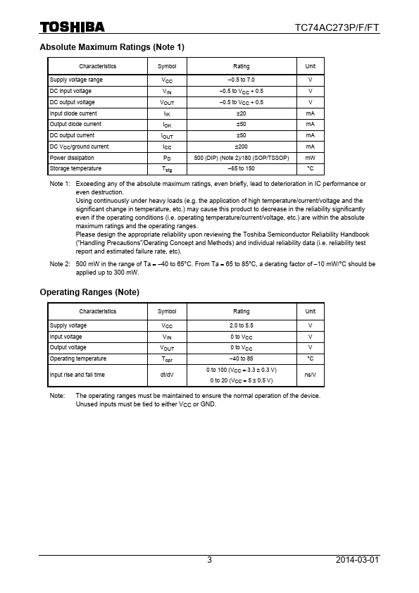 Page 3
TC74AC273FW Key Features
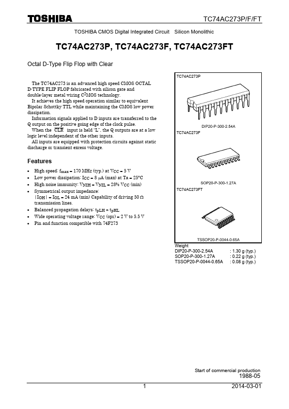
- High speed: fmax = 170 MHz (typ.) at VCC = 5 V
- Low power dissipation: ICC = 8 µA (max) at Ta = 25°C
- High noise immunity: VNIH = VNIL = 28% VCC (min)
- Symmetrical output impedance
- Balanced propagation delays: tpLH ∼- tpHL
- Wide operating voltage range: VCC (opr) = 2 V to 5.5 V
- Pin and function patible with 74F273
Other TC74AC273FW Datasheets
| Manufacturer |
Part Number |
Description |
 Toshiba
 |
TC74AC273F
|
Octal D-Type Flip-Flop |
|
Toshiba |
TC74AC273P
|
Octal D-Type Flip-Flop |