• Part: TC74VCX00FK
  • Description: Low-Voltage Quad 2-Input NAND Gate
  • Manufacturer: Toshiba
  • Size: 201.26 KB
Download TC74VCX00FK Datasheet PDF
TC74VCX00FK page 2
Page 2
TC74VCX00FK page 3
Page 3

TC74VCX00FK Datasheet Text

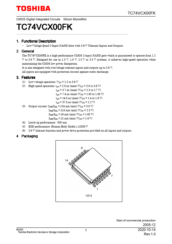
CMOS Digital Integrated Circuits Silicon Monolithic TC74VCX00FK TC74VCX00FK 1. Functional Description - Low-Voltage Quad 2-Input NAND Gate with 3.6-V Tolerant Inputs and Outputs 2. General The TC74VCX00FK is a high-performance CMOS 2-input NAND gate which is guaranteed to operate from 1.2 V to 3.6 V. Designed for use in 1.5 V, 1.8 V, 2.5 V or 3.3 V systems, it achieves high-speed operation while maintaining the CMOS low power dissipation. It is also designed with overvoltage tolerant inputs and outputs up to 3.6 V. All inputs are equipped with protection circuits against static discharge. 3. Features (1) Low-voltage operation: VCC = 1.2 to 3.6 V (2) High-speed operation: tpd = 2.8 ns (max) (VCC = 3.0 to 3.6 V) tpd = 3.7 ns (max) (VCC = 2.3 to 2.7 V) tpd = 7.4 ns (max) (VCC = 1.65 to 1.95 V) tpd = 14.8 ns (max) (VCC = 1.4 to 1.6 V) tpd = 37.0 ns (max) (VCC = 1.2 V) (3) Output current: IOH/IOL = ±24 mA (min) (VCC = 3.0 V) IOH/IOL = ±18 mA (min) (VCC = 2.3 V) IOH/IOL = ±6 mA (min) (VCC = 1.65 V) IOH/IOL = ±2 mA (min) (VCC = 1.4 V) (4) Latch-up performance: -300 mA (5) ESD performance: Human Body Model ≥ ±2000 V (6) 3.6 V tolerant function and power-down protection provided on all inputs and outputs. 4. Packaging US14 ©2020 Toshiba Electronic Devices & Storage Corporation 1 Start of mercial production 2005-12 2020-10-14 Rev.1.0 5. Pin Assignment TC74VCX00FK 6. Marking 7. IEC Logic Symbol ©2020 Toshiba Electronic Devices & Storage Corporation 2 2020-10-14 Rev.1.0 8. Truth Table Inputs A L L H H Inputs B L H L H Outputs Y H H H L 9....