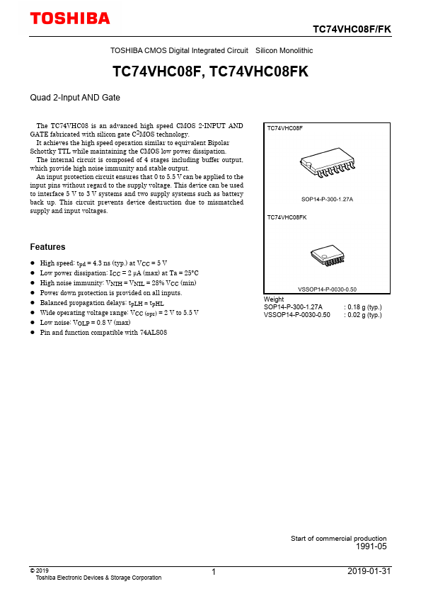
Datasheet4U Logo Datasheet4U.com

TC74VHC08FK - Quad 2-Input AND Gate

This page provides the datasheet information for the TC74VHC08FK, a member of the TC74VHC08FT Quad 2-Input AND Gate family.

Features

  • High speed: tpd = 4.3 ns (typ. ) at VCC = 5 V.
  • Low power dissipation: ICC = 2 μA (max) at Ta = 25°C.
  • High noise immunity: VNIH = VNIL = 28% VCC (min).
  • Power down protection is provided on all inputs.
  • Balanced propagation delays: tpLH ∼.
  • tpHL.
  • Wide operating voltage range: VCC (opr) = 2 V to 5.5 V.
  • Low noise: VOLP = 0.8 V (max).
  • Pin and function compatible with 74ALS08 Weight SOP14-P-300-1.27A VSSOP14-P-0030-0.50 : 0.18 g (typ. ) : 0.02 g (typ. ).

📥 Download Datasheet

Datasheet preview – TC74VHC08FK

Datasheet Details

Part number TC74VHC08FK
Manufacturer Toshiba
File Size 283.51 KB
Description Quad 2-Input AND Gate
Datasheet download datasheet TC74VHC08FK Datasheet
Additional preview pages of the TC74VHC08FK datasheet.
Other Datasheets by Toshiba

Full PDF Text Transcription

Click to expand full text
TC74VHC08F/FK TOSHIBA CMOS Digital Integrated Circuit Silicon Monolithic TC74VHC08F, TC74VHC08FK Quad 2-Input AND Gate The TC74VHC08 is an advanced high speed CMOS 2-INPUT AND GATE fabricated with silicon gate C2MOS technology. It achieves the high speed operation similar to equivalent Bipolar Schottky TTL while maintaining the CMOS low power dissipation. The internal circuit is composed of 4 stages including buffer output, which provide high noise immunity and stable output. An input protection circuit ensures that 0 to 5.5 V can be applied to the input pins without regard to the supply voltage. This device can be used to interface 5 V to 3 V systems and two supply systems such as battery back up. This circuit prevents device destruction due to mismatched supply and input voltages.
Published: |