TC74VHC11FN
Features
- High speed: tpd = 4.1 ns (typ.) at VCC = 5 V
- Low power dissipation: ICC = 2 μA (max) at Ta = 25°C
- High noise immunity: VNIH = VNIL = 28% VCC (min)
- Power down protection is provided on all inputs.
- Balanced propagation delays: tp LH ∼- tp HL
- Wide operating voltage range: VCC (opr) = 2 to 5.5 V
- Pin and function patible with 74ALS11
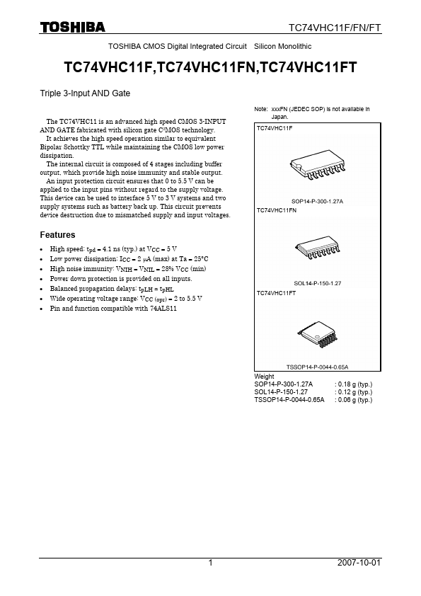
Note: xxx FN (JEDEC SOP) is not available in Japan.
TC74VHC11F
TC74VHC11FT
Weight SOP14-P-300-1.27A SOL14-P-150-1.27 TSSOP14-P-0044-0.65A
: 0.18 g (typ.) : 0.12 g (typ.) : 0.06 g (typ.)
1 2007-10-01
Pin Assignment
TC74VHC11F/FN/FT
IEC Logic Symbol
1A 1 1B 2 2A 3 2B 4 2C 5 2Y 6 GND 7
(top view)
14 VCC 13 1C 12 1Y 11 3C 10 3B 9 3A 8 3Y
1A (1) 1B (2) 1C (13) 2A (3) 2B (4) 2C (5) 3A (9) 3B (10) 3C (11)
&
(12) 1Y (6) 2Y (8) 3Y
Truth Table
LXX XLX XXL HHH
X: Don’t care
Absolute Maximum Ratings (Note)
Characteristics
Symbol
Rating
Unit
Supply voltage range DC input voltage DC output voltage Input...