TC74VHC273FW
Features
- High speed: fmax = 165 MHz (typ.) at VCC = 5 V
- Low power dissipation: ICC = 4 µA (max) at Ta = 25°C
- High noise immunity: VNIH = VNIL = 28% VCC (min)
- Power down protection is provided on all inputs.
- Balanced propagation delays: tp LH ∼- tp HL
- Wide operating voltage range: VCC (opr) = 2 to 5.5 V
- Low noise: VOLP = 0.9 V (max)
- Pin and function patible with 74ALS273
Note: xxx FW (JEDEC SOP) is not available in Japan.
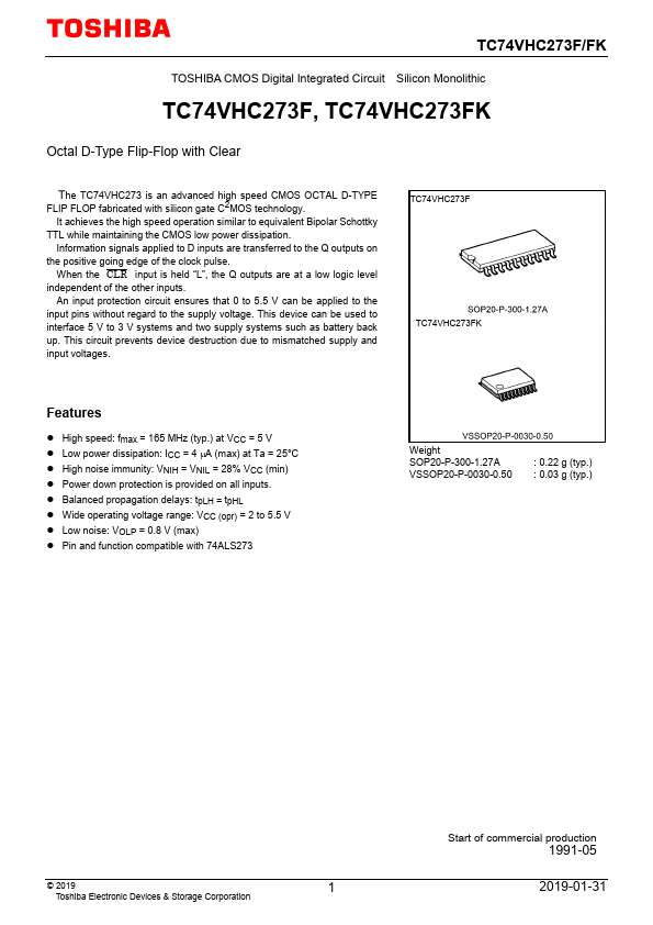
TC74VHC273F
TC74VHC273FT
TC74VHC273FK
Weight
SOP20-P-300-1.27A
: 0.22 g (typ.)
SOP20-P-300-1.27
: 0.22 g (typ.)
SOL20-P-300-1.27
: 0.46 g (typ.)
TSSOP20-P-0044-0.65A : 0.08 g (typ.)
VSSOP20-P-0030-0.50 : 0.03 g (typ.)
1 2006-06-01
Pin Assignment
TC74VHC273F/FW/FT/FK
IEC Logic Symbol
CLR 1 Q1 2 D1 3 D2 4 Q2 5 Q3 6 D3 7 D4 8 Q4 9
GND 10
(top view)
20 VCC 19 Q8 18 D8 17 D7 16 Q7 15 Q6 14 D6 13 D5 12 Q5 11 CK
Truth Table
Inputs CLR D
LX HL HH HX
CK X
X: Don’t care
Output Q L L H Qn
Function
Clear ― ―
No Change
System...