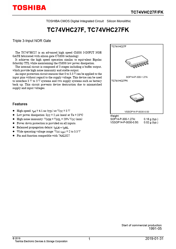
Download TC74VHC27FT Datasheet PDF
TC74VHC27FT page 2
Page 2
TC74VHC27FT page 3
Page 3

TC74VHC27FT Description

It achieves the high speed operation similar to equivalent Bipolar Schottky TTL while maintaining the CMOS low power dissipation. The internal circuit is posed of 3 stages including a buffer output, which provide high noise immunity and stable output. An input protection circuit ensures that 0 to 5.5 V can be applied to the input pins without regard to the supply voltage.

TC74VHC27FT Key Features

  • High speed: tpd = 4.1 ns (typ.) at VCC = 5 V
  • Low power dissipation: ICC = 2 μA (max) at Ta = 25°C
  • High noise immunity: VNIH = VNIL = 28% VCC (min)
  • Power down protection is provided on all inputs
  • Balanced propagation delays: tpLH ∼- tpHL
  • Wide operating voltage range: VCC (opr) = 2 to 5.5 V
  • Pin and function patible with 74ALS27