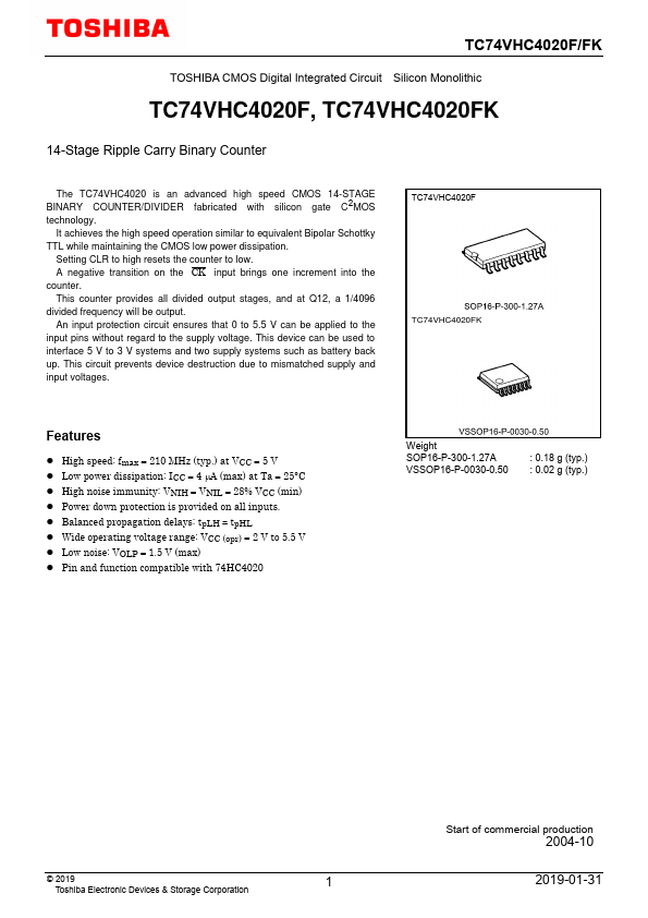
Datasheet4U Logo Datasheet4U.com

TC74VHC4020FK - 14-Stage Ripple Carry Binary Counter

Download the TC74VHC4020FK datasheet PDF. This datasheet also covers the TC74VHC4020F variant, as both devices belong to the same 14-stage ripple carry binary counter family and are provided as variant models within a single manufacturer datasheet.

Key Features

  • High speed: fmax  210 MHz (typ. ) at VCC  5 V.
  • Low power dissipation: ICC  4 A (max) at Ta  25°C.
  • High noise immunity: VNIH  VNIL  28% VCC (min).
  • Power down protection is provided on all inputs.
  • Balanced propagation delays: tpLH tpHL.
  • Wide operating voltage range: VCC (opr)  2 V to 5.5 V.
  • Low noise: VOLP  1.5 V (max).
  • Pin and function compatible with 74HC4020 Weight SOP16-P-300-1.27A VSSOP16-P-0030-0.50 : 0.18 g (typ. ) : 0.02 g (typ. ) © 20.

📥 Download Datasheet

Note: The manufacturer provides a single datasheet file (TC74VHC4020F-Toshiba.pdf) that lists specifications for multiple related part numbers.

Datasheet Details

Part number TC74VHC4020FK
Manufacturer Toshiba
File Size 359.05 KB
Description 14-Stage Ripple Carry Binary Counter
Datasheet download datasheet TC74VHC4020FK Datasheet

Full PDF Text Transcription for TC74VHC4020FK (Reference)

Note: Below is a high-fidelity text extraction (approx. 800 characters) for TC74VHC4020FK. For precise diagrams, and layout, please refer to the original PDF.

TC74VHC4020F/FK TOSHIBA CMOS Digital Integrated Circuit Silicon Monolithic TC74VHC4020F, TC74VHC4020FK 14-Stage Ripple Carry Binary Counter The TC74VHC4020 is an advanced...

View more extracted text
FK 14-Stage Ripple Carry Binary Counter The TC74VHC4020 is an advanced high speed CMOS 14-STAGE BINARY COUNTER/DIVIDER fabricated with silicon gate C2MOS technology. It achieves the high speed operation similar to equivalent Bipolar Schottky TTL while maintaining the CMOS low power dissipation. Setting CLR to high resets the counter to low. A negative transition on the CK input brings one increment into the counter. This counter provides all divided output stages, and at Q12, a 1/4096 divided frequency will be output. An input protection circuit ensures that 0 to 5.5 V can be applied to the input pins without regard to the