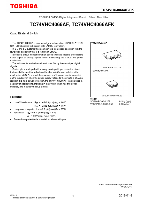
TC74VHC4066AF
feature of CMOS.
It consists of four independent high speed switches capable of controlling either digital or analog signals while maintaining the CMOS low power dissipation.
The switches for each channel are turned ON by the control pin digital signals.
Control pin is equipped with a newly developed input protection circuit that avoids the need for a diode on the plus side (forward side from the input to the VCC). As a result, for example, 5.5 V signals can be permitted on the inputs even when the power supply voltage to the circuits is off. As a result of this input power protection, the TC74VHC4066AFT can be used in a variety of applications, including in the system which has two power supplies, and in battery backup circuits.
TC74VHC4066AF TC74VHC4066AFK
Features
- Low ON resistance: Ron = 45 Ω (typ.) (VCC = 3.0 V) Ron = 24 Ω (typ.) (VCC = 4.5 V)
- Low power dissipation: ICC = 2.0 μA (max) (Ta = 25°C)
- Input level: VIL = 0.8 V (max) (VCC = 3 V)
VIH = 2.0 V (min) (VCC = 3 V)
-...


