Datasheet4U Logo Datasheet4U.com
Toshiba logo

TC74VHCT32AFN

Manufacturer: Toshiba

TC74VHCT32AFN datasheet PDF for QUAD 2-INPUT OR GATE.

TC74VHCT32AFN datasheet preview

TC74VHCT32AFN Datasheet Details

Part number TC74VHCT32AFN
Datasheet TC74VHCT32AFN_ToshibaSemiconductor.pdf
File Size 203.99 KB
Manufacturer Toshiba
Description QUAD 2-INPUT OR GATE
TC74VHCT32AFN page 2 TC74VHCT32AFN page 3

TC74VHCT32AFN Overview

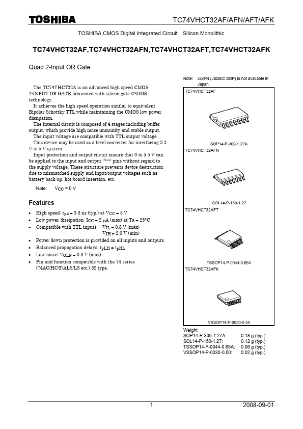
It achieves the high speed operation similar to equivalent Bipolar Schottky TTL while maintaining the CMOS low power dissipation. The internal circuit is posed of 4 stages including buffer output, which provide high noise immunity and stable output. The input voltage are patible with TTL output voltage.

TC74VHCT32AFN Key Features

  • High speed: tpd = 3.8 ns (typ.) at VCC = 5 V
  • Low power dissipation: ICC = 2 μA (max) at Ta = 25°C
  • patible with TTL inputs: VIL = 0.8 V (max)
  • Power down protection is provided on all inputs and outputs
  • Balanced propagation delays: tpLH ∼- tpHL
  • Low noise: VOLP = 0.8 V (max)
  • Pin and function patible with the 74 series
Toshiba logo - Manufacturer

More Datasheets from Toshiba

See all Toshiba datasheets

Part Number Description
TC74VHCT32AF Quad 2-Input OR Gate
TC74VHCT32AFK Quad 2-Input OR Gate
TC74VHCT32AFT QUAD 2-INPUT OR GATE
TC74VHCT367AF Hex Bus Buffer
TC74VHCT367AFN HEX BUS BUFFER
TC74VHCT367AFT Hex Bus Buffer
TC74VHCT373AF Octal D-Type Latch
TC74VHCT373AFK Octal D-Type Latch
TC74VHCT373AFT Octal D-Type Latch
TC74VHCT373AFW OCTAL D-TYPE LATCH WITH 3-STATE OUTPUT

TC74VHCT32AFN Distributor

Datasheet4U Logo
Since 2006. D4U Semicon. About Datasheet4U Contact Us Privacy Policy Purchase of parts