TC74VHCT74AFN
Features
- High speed: fmax = 160 MHz (typ.) at VCC = 5 V
- Low power dissipation: ICC = 2 μA (max) at Ta = 25°C
- patible with TTL inputs: VIL = 0.8 V (max)
VIH = 2.0 V (min)
- Power down protection is provided on all inputs and outputs
- Balanced propagation delays: tp LH ≈ tp HL
- Pin and function patible with the 74 series
(74AC/HC/F/ALS/LS etc.) 74 type.
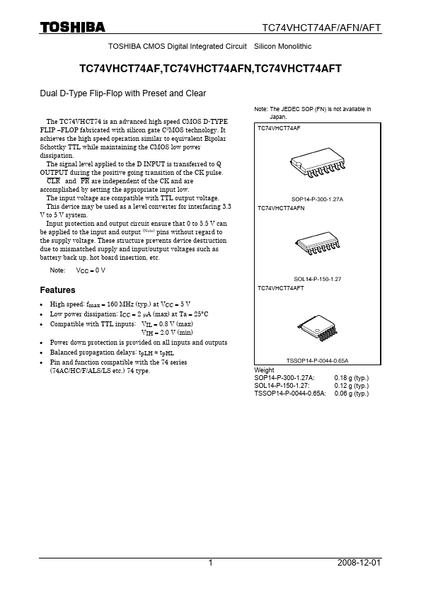
Note: The JEDEC SOP (FN) is not available in Japan.
TC74VHCT74AF
TC74VHCT74AFT
Weight SOP14-P-300-1.27A: SOL14-P-150-1.27: TSSOP14-P-0044-0.65A:
0.18 g (typ.) 0.12 g (typ.) 0.06 g (typ.)
1 2008-12-01
Pin Assignment
TC74VHCT74AF/AFN/AFT
IEC Logic Symbol
1CLR 1 1D 2
1CK 3 1PR 4
1Q 5 1Q 6 GND 7
CK D QQ
CK D QQ
14 VCC 13 2CLR 12 2D 11 2CK 10 2PR 9 2Q 8 2Q
1PR 1CK
1D 1CLR
2PR 2CK
2D 2CLR
(4) (3) (2) (1) (10) (11) (12) (13)
S C1
1D R
(5) 1Q (6) 1Q (9) 2Q (8) 2Q
(top view)
Truth Table
CLR L H L H H H
Inputs
PR D HX LX LX HL HH HX
X: Don’t care
Outputs
CK...