Datasheet4U Logo Datasheet4U.com

TC7MBL3126CFK - Low-Voltage Low-Capacitance Quad Bus Switch

Download the TC7MBL3126CFK datasheet PDF. This datasheet also covers the TC7MBL3125CFK variant, as both devices belong to the same low-voltage low-capacitance quad bus switch family and are provided as variant models within a single manufacturer datasheet.

General Description

2.

The TC7MBL3125CFK and TC7MBL3126CFK are a low-voltage/low-capacitance CMOS 4bit Bus Switch.

The low on-resistance of the switch allows connections to be made with minimal propagation delay time.

Key Features

  • (1) Operating voltage: VCC = 1.65 to 3.6 V (2) ON capacitance: CI/O = 7.5 pF Switch On (typ. ) @VCC = 3.0 V (3) ON resistance: RON = 6.5 Ω (typ. ) @VCC = 3.0 V, VIS = 0 V (4) ESD performance: MM ≥ ±200 V, HBM ≥ ±2000 V (5) Power-down protection for inputs (OE, OE and I/O) (6) Package: VSSOP14 (US14) 4. 
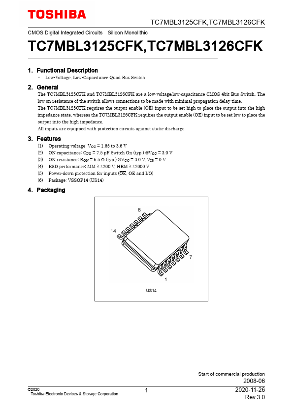
Packaging US14 ©2020 1 Toshiba Electronic Devices & Storage Corporation Start of commercial production 2008-06 2020-11-26 Rev.3.0 5. Pin Assignment TC7MBL3125CFK TC7MBL3125CFK,TC7MBL3126CFK T.

📥 Download Datasheet

Note: The manufacturer provides a single datasheet file (TC7MBL3125CFK-Toshiba.pdf) that lists specifications for multiple related part numbers.

Datasheet Details

Part number TC7MBL3126CFK
Manufacturer Toshiba
File Size 270.72 KB
Description Low-Voltage Low-Capacitance Quad Bus Switch
Datasheet download datasheet TC7MBL3126CFK Datasheet

Full PDF Text Transcription (Reference)

The following content is an automatically extracted verbatim text from the original manufacturer datasheet and is provided for reference purposes only.

View original datasheet text
TC7MBL3125CFK,TC7MBL3126CFK CMOS Digital Integrated Circuits Silicon Monolithic TC7MBL3125CFK,TC7MBL3126CFK 1. Functional Description • Low-Voltage, Low-Capacitance Quad Bus Switch 2. General The TC7MBL3125CFK and TC7MBL3126CFK are a low-voltage/low-capacitance CMOS 4bit Bus Switch. The low on-resistance of the switch allows connections to be made with minimal propagation delay time. The TC7MBL3125CFK requires the output enable (OE) input to be set high to place the output into the high impedance state, whereas the TC7MBL3126CFK requires the output enable (OE) input to be set low to place the output into the high impedance. All inputs are equipped with protection circuits against static discharge. 3. Features (1) Operating voltage: VCC = 1.65 to 3.6 V (2) ON capacitance: CI/O = 7.