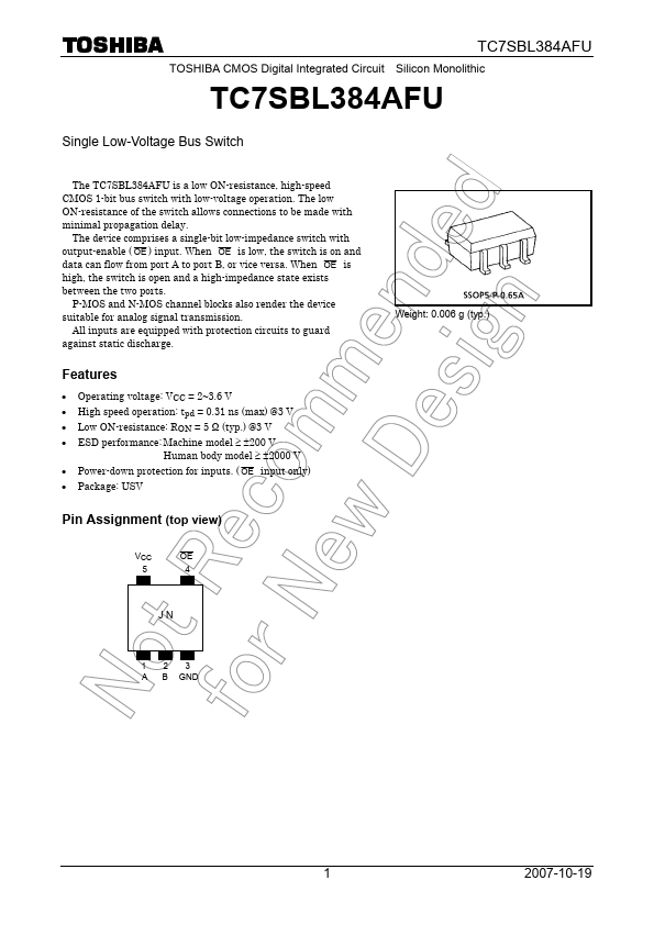
ESD performance: Machine model ≥ ±200 V
Human body model ≥ ±2000 V.
Power-down protection for inputs. ( OE input only).
Package: USV
Pin Assignment (top view)
VCC
OE
5
4
Weight: 0.006 g (typ. )
JN
123 A B GND
1
2007-10-19
Truth Table
Input OE L H
Function A port = B port Disconnect
System Diagram
TC7SBL384A.
Full PDF Text Transcription for TC7SBL384AFU (Reference)
Note: Below is a high-fidelity text extraction (approx. 800 characters) for
TC7SBL384AFU. For precise diagrams, and layout, please refer to the original PDF.
TC7SBL384AFU TOSHIBA CMOS Digital Integrated Circuit Silicon Monolithic TC7SBL384AFU Single Low-Voltage Bus Switch The TC7SBL384AFU is a low ON-resistance, high-speed CMO...
View more extracted text
age Bus Switch The TC7SBL384AFU is a low ON-resistance, high-speed CMOS 1-bit bus switch with low-voltage operation. The low ON-resistance of the switch allows connections to be made with minimal propagation delay. The device comprises a single-bit low-impedance switch with output-enable ( OE ) input. When OE is low, the switch is on and data can flow from port A to port B, or vice versa. When OE is high, the switch is open and a high-impedance state exists between the two ports. P-MOS and N-MOS channel blocks also render the device suitable for analog signal transmission. All inputs are equipped with protection circuits t