TC7SG04FE
Features
- High output current
: ±8 m A (min) at VCC = 3.0 V
- Super high speed operation : tpd = 2.3 ns (typ.) at VCC = 3.3 V,15p F
- Operating voltage range : VCC = 0.9 to 3.6 V
- 5.5-V tolerant input
- 3.6-V power down protection output
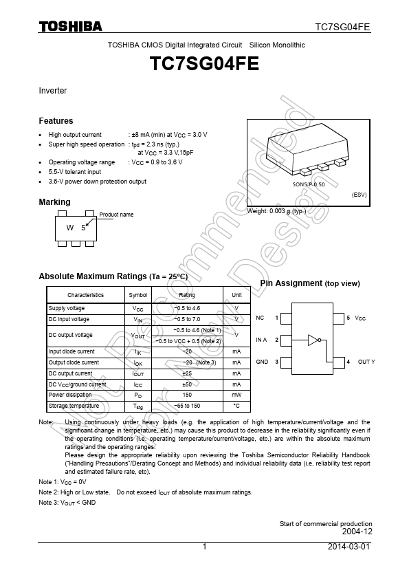
Marking
W5
Product name
Weight: 0.003 g (typ.)
(ESV)
Absolute Maximum Ratings (Ta = 25°C)
Characteristics
Symbol
Rating
Pin Assignment (top view)
Unit
Supply voltage DC input voltage
DC output voltage
Input diode current Output diode current DC output current DC VCC/ground current Power dissipation Storage temperature
- 0.5 to 4.6
- 0.5 to 7.0
- 0.5 to 4.6 (Note 1)
VOUT
- 0.5 to VCC + 0.5 (Note 2)
IIK IOK IOUT
- 20 m A
- 20 (Note 3) m A
±25 m A
±50 m A
150 m...