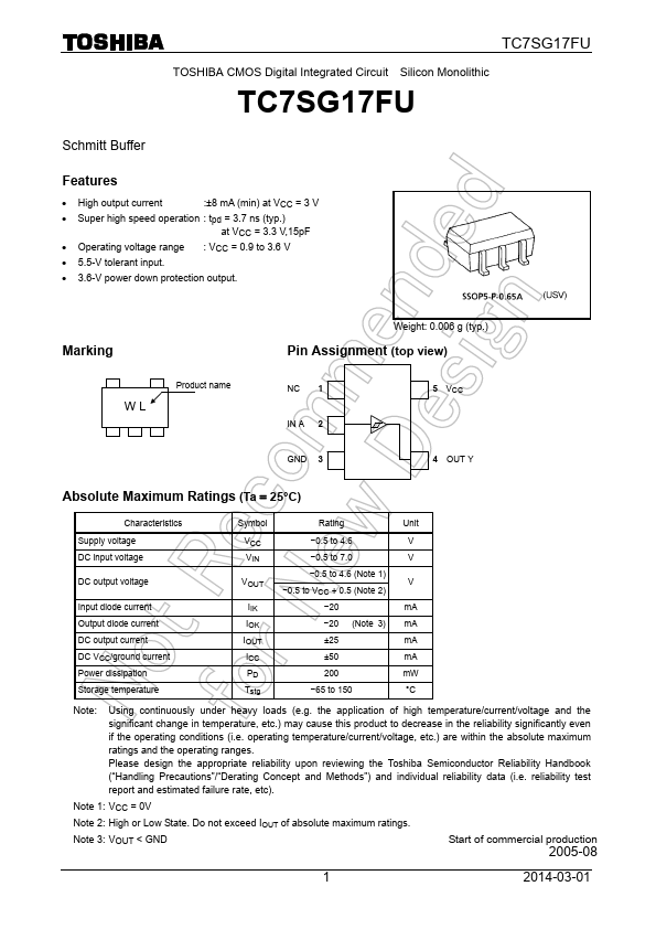
Super high speed operation : tpd = 3.7 ns (typ. ) at VCC = 3.3 V,15pF.
Operating voltage range : VCC = 0.9 to 3.6 V.
5.5-V tolerant input.
3.6-V power down protection output. Marking
Weight: 0.006 g (typ. )
Pin Assignment (top view)
WL
Product name
NC 1 IN A 2
5 VCC
GND 3
4 OUT Y
Absolute Maximum Ratings (Ta = 25°C)
Characteristics
Symbol
Rating
Unit
Supply voltage DC input voltage
DC.
Full PDF Text Transcription for TC7SG17FU (Reference)
Note: Below is a high-fidelity text extraction (approx. 800 characters) for
TC7SG17FU. For precise diagrams, and layout, please refer to the original PDF.
TC7SG17FU TOSHIBA CMOS Digital Integrated Circuit Silicon Monolithic TC7SG17FU Schmitt Buffer Features • High output current :±8 mA (min) at VCC = 3 V • Super high speed ...
View more extracted text
es • High output current :±8 mA (min) at VCC = 3 V • Super high speed operation : tpd = 3.7 ns (typ.) at VCC = 3.3 V,15pF • Operating voltage range : VCC = 0.9 to 3.6 V • 5.5-V tolerant input. • 3.6-V power down protection output. Marking Weight: 0.006 g (typ.) Pin Assignment (top view) WL Product name NC 1 IN A 2 5 VCC GND 3 4 OUT Y Absolute Maximum Ratings (Ta = 25°C) Characteristics Symbol Rating Unit Supply voltage DC input voltage DC output voltage Input diode current Output diode current DC output current DC VCC/ground current Power dissipation Storage temperature VCC VIN VOUT IIK IOK IOUT ICC PD Tstg −0.5 to 4.6 V −