Datasheet4U Logo Datasheet4U.com

TC7SZ08 - 2 INPUT AND GATE

Features

  • High output drive: ±24 mA (typ. ) @VCC = 3 V.
  • Super high speed operation: tPD 2.7 ns (typ. ) @VCC = 5 V, 50 pF.
  • Operation voltage range: VCC (opr) = 1.8~5.5 V.
  • Supply voltage data retention: VCC = 1.5~5.5 V.
  • Latch-up performance: ±500 mA.
  • ESD performance: Human body model > ±2000 V Machine model > ±200 V Weight: 0.003 g (typ. ).
  • Power down protection is provided on all inputs.
  • Matches the performance of TC74LCX series when operated at 3.3 V VCC.

📥 Download Datasheet

Datasheet preview – TC7SZ08

Datasheet Details

Part number TC7SZ08
Manufacturer Toshiba
File Size 86.83 KB
Description 2 INPUT AND GATE
Datasheet download datasheet TC7SZ08 Datasheet
Additional preview pages of the TC7SZ08 datasheet.
Other Datasheets by Toshiba

Full PDF Text Transcription

Click to expand full text
TC7SZ08AFE TOSHIBA CMOS Digital Integrated Circuit Silicon Monolithic TC7SZ08AFE 2 Input AND Gate Features · High output drive: ±24 mA (typ.) @VCC = 3 V · Super high speed operation: tPD 2.7 ns (typ.) @VCC = 5 V, 50 pF · Operation voltage range: VCC (opr) = 1.8~5.5 V · Supply voltage data retention: VCC = 1.5~5.5 V · Latch-up performance: ±500 mA · 
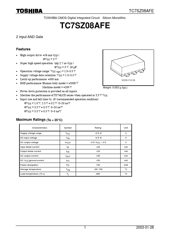
ESD performance: Human body model > ±2000 V Machine model > ±200 V Weight: 0.003 g (typ.) · Power down protection is provided on all inputs. · Matches the performance of TC74LCX series when operated at 3.3 V VCC · Input rise and fall time (tr, tf) (recommended operation condition) @VCC = 1.8 V, 2.5 V ± 0.2 V: 0~20 ns/V @VCC = 3.3 V ± 0.3 V: 0~10 ns/V @VCC = 5.5 V ± 0.
Published: |