TC7USB221WBG
Description
- Dual SPDT USB Switch
2. General
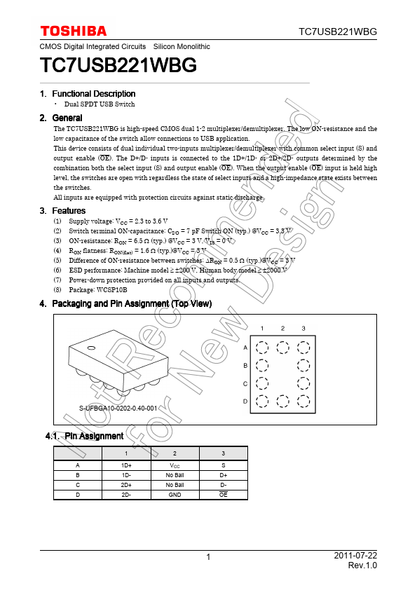
The TC7USB221WBG is high-speed CMOS dual 1-2 multiplexer/demultiplexer. The low ON-resistance and the low capacitance of the switch allow connections to USB application. This device consists of dual individual two-inputs multiplexer/demultiplexer with mon select input (S) and output enable (OE). The D+/D- inputs is connected to the 1D+/1D- or 2D+/2D- outputs determined by the bination both the select input (S) and output enable (OE). When the output enable (OE) input is held high level, the switches are open with regardless the state of select inputs and a high-impedance state exists between the switches. All inputs are equipped with protection circuits against static discharge.
3. Features
(1) Supply voltage: VCC = 2.3 to 3.6 V (2) Switch terminal ON-capacitance: CI/O = 7 p F Switch ON (typ.) @VCC = 3.3 V (3) ON-resistance: RON = 6.5 Ω (typ.) @VCC = 3 V, VIS = 0 V (4) RON flatness: RON(flat) = 1.6 Ω (typ.)@VCC = 3 V (5) Difference of...