TC7WBL125AFK
TC7WBL125AFK is Low-Voltage Dual Bus Switch manufactured by Toshiba.
TOSHIBA CMOS Digital Integrated Circuit Silicon Monolithic
Low-Voltage Dual Bus Switch
The TC7WBL125AFK provides two bits of low-voltage, high-speed bus switching. The low ON-resistance of the switch allows connections to be made with minimal propagation delay and while maintaining CMOS low power dissipation.
The device prises dual 2-bit switches with separate bus enable ( OE ) signals. When OE is low, the switch is on and port A is connected to port B. When OE is high, the switch is off and a high-impedance state exists between the two ports.
All inputs are equipped with protection circuits to guard against static discharge.
Features
- Operating voltage range: VCC = 2 to 3.6 V
- High speed: tpd = 0.31 ns (max) @ 3 V
- Ultra-low ON-resistance: RON = 5 Ω (typ.) @ 3 V
- ESD performance: Machine model ≥ ±200 V
Human body model ≥ ±2000 V
- Power-down protection provided on inputs ( OE input only)
- Package: US8
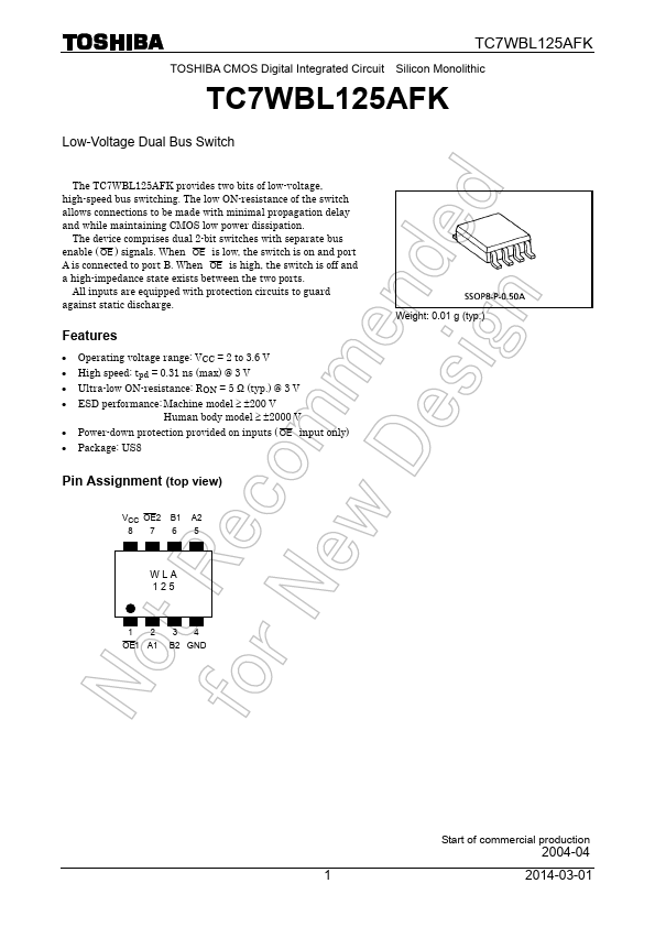
Pin Assignment (top view)
VCC OE2 B1 A2 8765
Weight: 0.01 g (typ.)
WLA 125
12 34 OE1 A1 B2 GND
Start of mercial production
2004-04
2014-03-01
Truth Table
Inputs OE L H
Function
A port = B port Disconnect
Logic Diagram
A1
B1
A2
B2...