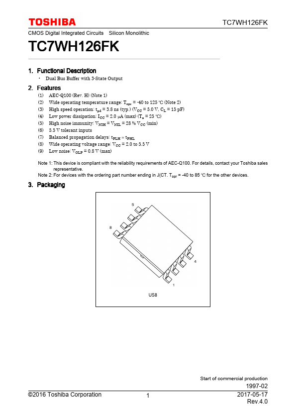
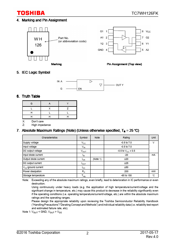
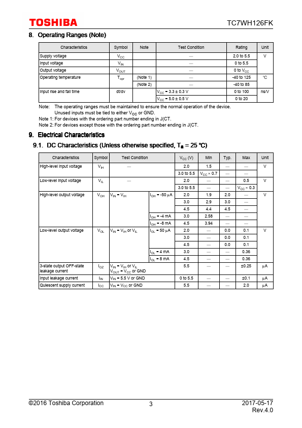
Datasheet4U Logo Datasheet4U.com

TC7WH126FK - Dual BUS Buffer

General Description

2.

Key Features

  • (1) AEC-Q100 (Rev. H) (Note 1) (2) Wide operating temperature range: Topr = -40 to 125  (Note 2) (3) High speed operation: tpd = 3.8 ns (typ. ) (VCC = 5.0 V, CL = 15 pF) (4) Low power dissipation: ICC = 2.0 µA (max) (Ta = 25 ) (5) High noise immunity: VNIH = VNIL = 28 % VCC (min) (6) 5.5 V tolerant inputs (7) Balanced propagation delays: tPLH ≈ tPHL (8) Wide operating voltage range: VCC = 2.0 to 5.5 V (9) Low noise: VOLP = 0.8 V (max) Note 1: This device is compliant with the reliability requir.

📥 Download Datasheet

Full PDF Text Transcription (Reference)

The following content is an automatically extracted verbatim text from the original manufacturer datasheet and is provided for reference purposes only.

View original datasheet text
CMOS Digital Integrated Circuits Silicon Monolithic TC7WH126FK TC7WH126FK 1. Functional Description • Dual Bus Buffer with 3-State Output 2. Features (1) AEC-Q100 (Rev. H) (Note 1) (2) Wide operating temperature range: Topr = -40 to 125  (Note 2) (3) High speed operation: tpd = 3.8 ns (typ.) (VCC = 5.0 V, CL = 15 pF) (4) Low power dissipation: ICC = 2.0 µA (max) (Ta = 25 ) (5) High noise immunity: VNIH = VNIL = 28 % VCC (min) (6) 5.5 V tolerant inputs (7) Balanced propagation delays: tPLH ≈ tPHL (8) Wide operating voltage range: VCC = 2.0 to 5.5 V (9) Low noise: VOLP = 0.8 V (max) Note 1: This device is compliant with the reliability requirements of AEC-Q100. For details, contact your Toshiba sales representative. Note 2: For devices with the ordering part number ending in J(CT.