Toshiba TD7104F
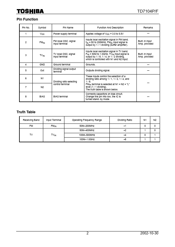
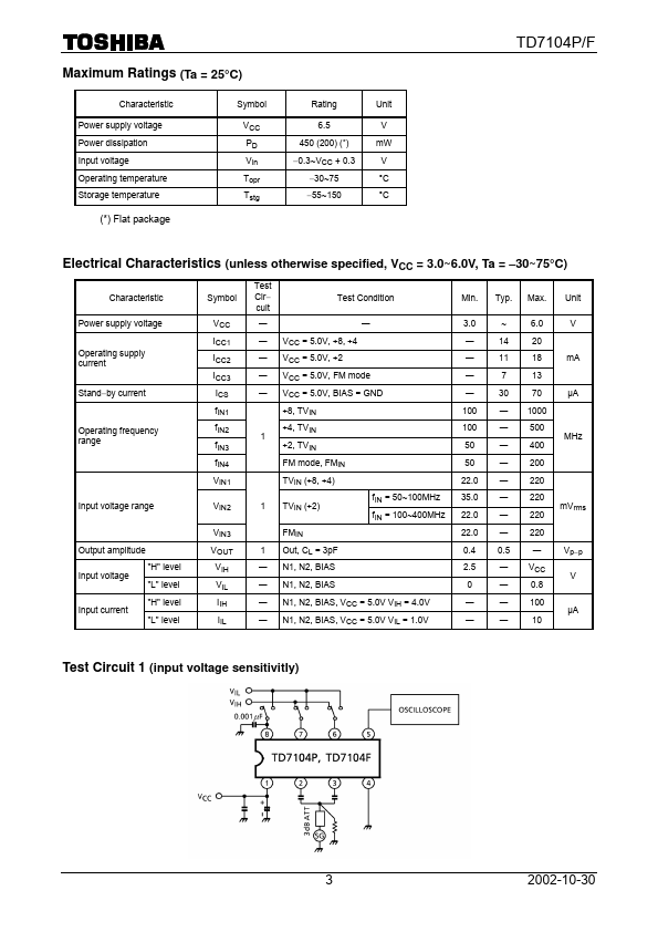
The truth table is shown below.| Part No. | TD7104F |
|---|---|
| Datasheet | TD7104F Download |
| Manufacturer |  Toshiba |
| Description | ECL PRESCALER |
| Buy | Stock & Price |
FEATURES
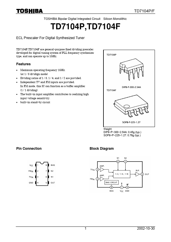
● Maximum operating frequency 1GHz. (at 1 / 8 dividign mode)● Dividing ratios of 1 / 8, 1 / 4, and 1 / 2 are provided.
● Independent TV and FM inputs are provided. In FM mode, this IC can function as a buffer amplifier (1 / 1 dividing).
● The built−in input amplifier contributes to realizing high input voltage sensitivity.
● built−in stand−by circuit Pin Connection Weight DIP8−P−300−2.54A: 0.45g (typ.) SOP8−P−225−1.27: 0.76g (typ.) Block Diagram 1 2002-10-30 Pin Function Pin No. 1 Symbol VCC 2 FMIN Pin Name Power supply terminal FM local OSC. signal input terminal 3 TVIN TV local OSC. signal input terminal 4 GND Ground terminal 5 Out Dividing signal output terminal 6 N1 Dividing ratio selecting control terminal 7 N2 8 BIAS BIAS terminal TD7104P/F Function And
DESCRIPTION
Applies voltage of VCC = 3.0 to 5.5V Inputs local oscillation signal in FM band. fIN = 50 to 200MHz, FMIN input signal is output by 1 / 1 dividing (buffer amplifier). Inputs local oscillation signal in TV band.