TJ11A10M3
TJ11A10M3 is manufactured by Toshiba.
MOSFETs Silicon P-Channel MOS (U-MOS)
1. Applications
- Switching Voltage Regulators
2. Features
(1) (2) (3) Low drain-source on-resistance: RDS(ON) = 100 mΩ (typ.) (VGS = -10 V) Low leakage current: IDSS = -10 µA (max) (VDS = -100 V) Enhancement mode: Vth = -2.0 to -4.0 V (VDS = -10 V, ID = -1 mA)
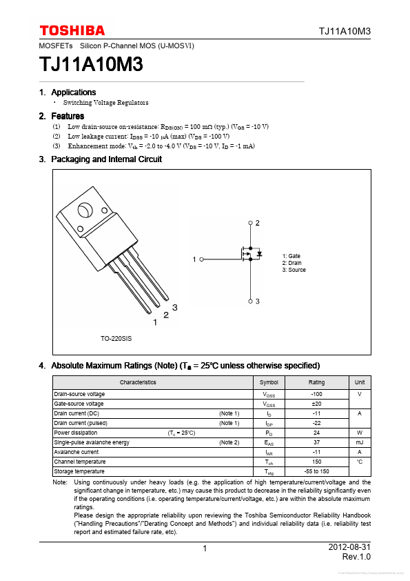
3. Packaging and Internal Circuit
1: Gate 2: Drain 3: Source
TO-220SIS
4....