(1) Low drain-source on-resistance: RDS(ON) = 0.11 Ω (typ. ) by used to Super Junction Structure : DTMOS
(2) High-speed switching properties with lower capacitance. (3) Enhancement mode: Vth = 2.5 to 3.5 V (VDS = 10 V, ID = 1.2 mA)
3. Packaging and Internal Circuit
TK25V60X
DFN8x8
1: Gate 2: Source1 3,4: Source2 5: Drain (Heatsink)
Notice: Please use the source1 pin for gate input signal return. Make sure that the main current flows into the source2 pins. 4. Absolute Maximum Ratings (Note) (T.
Full PDF Text Transcription for TK25V60X (Reference)
Note: Below is a high-fidelity text extraction (approx. 800 characters) for
TK25V60X. For precise diagrams, and layout, please refer to the original PDF.
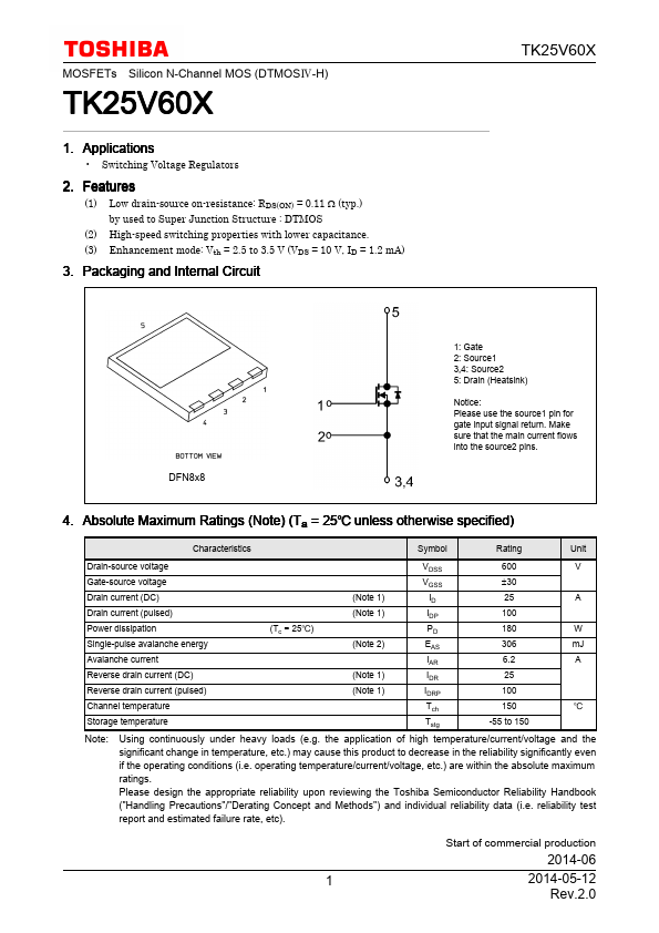
MOSFETs Silicon N-Channel MOS (DTMOS-H) TK25V60X 1. Applications • Switching Voltage Regulators 2. Features (1) Low drain-source on-resistance: RDS(ON) = 0.11 Ω (typ.) b...
View more extracted text
Features (1) Low drain-source on-resistance: RDS(ON) = 0.11 Ω (typ.) by used to Super Junction Structure : DTMOS (2) High-speed switching properties with lower capacitance. (3) Enhancement mode: Vth = 2.5 to 3.5 V (VDS = 10 V, ID = 1.2 mA) 3. Packaging and Internal Circuit TK25V60X DFN8x8 1: Gate 2: Source1 3,4: Source2 5: Drain (Heatsink) Notice: Please use the source1 pin for gate input signal return. Make sure that the main current flows into the source2 pins. 4.