TK3R1E04PL
Features
(1) High-speed switching (2) Small gate charge: QSW = 17.5 n C (typ.) (3) Small output charge: Qoss = 42 n C (typ.) (4) Low drain-source on-resistance: RDS(ON) = 2.5 mΩ (typ.) (VGS = 10 V) (5) Low leakage current: IDSS = 10 µA (max) (VDS = 40 V) (6) Enhancement mode: Vth = 1.4 to 2.4 V (VDS = 10 V, ID = 0.5 m A)
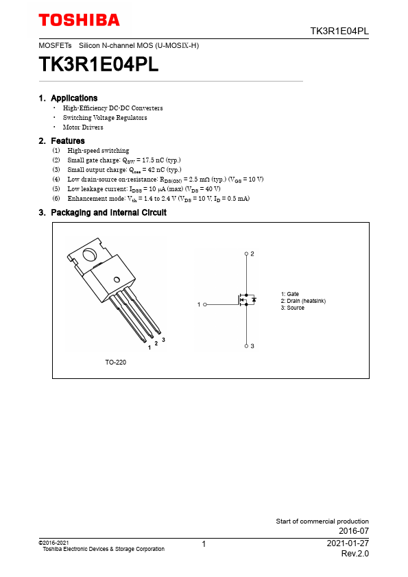
3. Packaging and Internal Circuit
TO-220
1: Gate 2: Drain (heatsink) 3: Source
©2016-2021
Toshiba Electronic Devices & Storage Corporation
Start of mercial production
2016-07
2021-01-27 Rev.2.0
4. Absolute Maximum Ratings (Note) (Ta = 25
- unless otherwise specified)
Characteristics
Symbol
Rating
Unit
Drain-source voltage Gate-source voltage Drain current (DC) Drain current (DC) Drain current (pulsed) Power dissipation Single-pulse avalanche energy Single-pulse avalanche current Channel temperature Storage temperature Mounting torque
(Tc = 25
- ) (Silicon limit) (t = 100 µs) (Tc = 25
- )
(Note 1) (Note 1), (Note 2)
(Note 1)
(Note 3)...