Silicon N Channel MOS Type Field Effect Transistor
Full PDF Text Transcription (Reference)
The following content is an automatically extracted verbatim text
from the original manufacturer datasheet and is provided for reference purposes only.
View original datasheet text
TK8A55DA
TOSHIBA Field Effect Transistor Silicon N Channel MOS Type (π-MOSⅦ)
TK8A55DA
Switching Regulator Applications
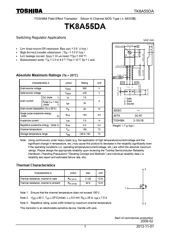
Ф3.2 ± 0.2 10 ± 0.3
Unit: mm
2.7 ± 0.2 A 3.9 3.0 1.14 ± 0.15 2.8 MAX. 2.54 1 2 3 2.6 ± 0.1 13 ± 0.5 0.69 ± 0.15 Ф0.2 M A
Absolute Maximum Ratings (Ta = 25°C)
Characteristics S Drain-source voltage Gate-source voltage DC (Note Drain current 1) ymbol VDSS VGSS ID IDP PD 2) EAS IAR EAR Tch Tstg Rating 550 ±30 7.5 30 40 163 7.5 4.0 150 −55 to 150 A W mJ A mJ °C °C Unit V V
2.54 0.64 ± 0.15
15.0 ± 0.3
• • • •
Low drain-source ON-resistance: RDS (ON) = 0.9 Ω(typ.) High forward transfer admittance: |Yfs| = 3.0 S (typ.) Low leakage current: IDSS = 10 μA (max) (VDS = 550 V) Enhancement mode: Vth = 2.0 to 4.