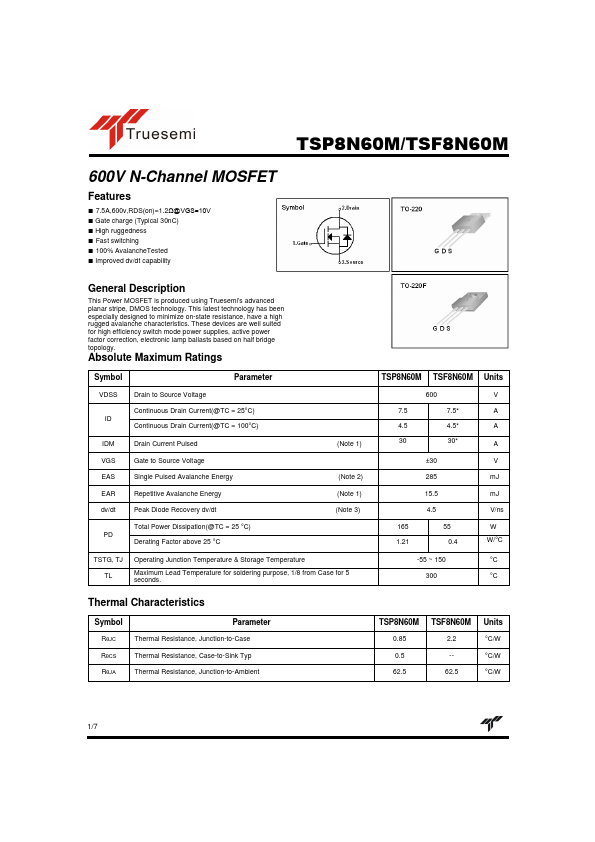
TSF8N60M
TSF8N60M is 600V N-Channel MOSFET manufactured by Truesemi.
Features
- 7.5A,600v,RDS(on)=1.2Ω@VGS=10V
- Gate charge (Typical 30n C)
- High ruggedness
- Fast switching
- 100% Avalanche Tested
- Improved dv/dt capability
General Description
This Power MOSFET is produced using Truesemi’s advanced planar stripe, DMOS technology. This latest technology has been especially designed to minimize on-state resistance, have a high rugged avalanche characteristics. These devices are well suited for high efficiency switch mode power supplies, active power factor correction, electronic lamp ballasts based on half bridge topology.
Absolute Maximum Ratings
Symbol
VDSS Drain to Source Voltage Continuous Drain Current(@TC = 25°C) ID Continuous Drain Current(@TC = 100°C) IDM VGS EAS EAR dv/dt Drain Current Pulsed Gate to Source Voltage Single Pulsed Avalanche Energy Repetitive Avalanche Energy Peak Diode Recovery dv/dt Total Power Dissipation(@TC = 25 °C) PD Derating Factor above 25 °C TSTG, TJ TL Operating Junction Temperature & Storage Temperature Maximum Lead Temperature for soldering purpose, 1/8 from Case for 5 seconds. 1.21 -55 ~ 150 300 0.4 (Note 2) (Note 1) (Note 3) 165 (Note 1) 4.5 30 ±30 285 15.5 4.5 55 4.5- 30- A A V m J m J V/ns W W/°C °C °C 7.5
Parameter
TSP8N60M
600 7.5-
Units
Thermal Characteristics
Symbol
RθJC RθCS RθJA
Parameter
Thermal Resistance, Junction-to-Case Thermal Resistance, Case-to-Sink Typ Thermal Resistance, Junction-to-Ambient
TSP8N60M
0.85 0.5 62.5
2.2 -62.5
Units
°C/W °C/W °C/W
1/7
TSP8N60M/TSF8N60M
Electrical Characteristics
Symbol Off Characteristics
BVDSS Δ BVDSS /Δ TJ IDSS Drain-Source Breakdown Voltage Breakdown Voltage Temperature coefficient Drain-Source Leakage Current VDS = 480V, TC = 125 °C Gate-Source Leakage, Forward IGSS Gate-source Leakage, Reverse VGS = -30V, VDS = 0V ---100 n A VGS = 30V, VDS = 0V ----100 100 u A n A VGS = 0V, ID = 250u A ID = 250u A, referenced to 25 °C VDS = 600V, VGS = 0V 600 ---0.57 ---10 V V/°C u A
( TC = 25 °C unless otherwise noted ) Test...