TTS3816B4E
TTS3816B4E is 2M x 16Bit x 4 Banks synchronous DRAM manufactured by TwinMOS.
DESCRIPTION
The TTS3816B4E is 134,217,728 bits synchronous high data rate Dynamic RAM organized as 8 x 1,048,576 words by 16 bits, fabricated with M’tec high performance CMOS technology. Synchronous design allows precise cycle control with the use of system clock I/O transactions are possible on every clock cycle. Range of operating frequencies, programmable burst length and programmable latencies allow the same device to be useful for a variety of high bandwidth, high performance memory system .. applications.
FEATURES
- JEDEC standard 3.3V power supply
- LVTTL patible with multiplexed address
- Four-banks operation
- MRS cycle with address key programs -. CAS latency (2 & 3) -. Burst length (1, 2, 4, 8 & Full page) -. Burst type (Sequential & Interleave)
- All inputs are sampled at the positive going edge of the system clock.
- Burst read single-bit write operation
- DQM for masking
- Auto & self refresh
- 64ms refresh period (4K cycle)
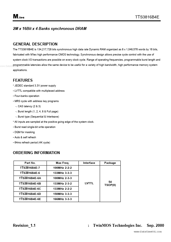
ORDERING INFORMATION
Part No. TTS3816B4E-7 TTS3816B4E-6 TTS3816B4E-6A TTS3816B4E-6B TTS3816B4E-6C TTS3816B4E-6D TTS3816B4E-6E Max Freq. 100MHz 2-2-2 133MHz 3-3-3 100MHz 2-3-3 133MHz 2-3-2 133MHz 2-2-2 150MHz 3-3-3 166MHz 3-3-3 LVTTL 54 TSOP(II) Interface Package
Revision_1.1
Twin MOS Technologies Inc.
Sep. 2000
M.tec
PIN CONFIGURATION (Top View)
..
54Pin TSOP (II) (400mil x 875mil) (0.8 mm Pin pitch)
Revision_1.1
Twin MOS Technologies Inc.
Sep. 2000
M.tec
PIN FUNCTION DESCRIPTION
Pin Name
A0~ A11 BS0, BS1 DQ0 ~DQ15 /CS .. /RAS /CAS /WE UDQM/LDQM CLK CKE Vcc Vss Vcc Vss NC Address Bank Data Input / Output Chip Select Row Address Strobe Column Address Strobe Write Enable Input /output mask Clock Input Clock Enable Power (+3.3 V) Ground
Function
Description
Multiplexed pins for row and column address Row address: A0 ~ A11. Column address: A0 ~ A8. Select bank to activate during row address latch time, or bank to read/write during address latch time. Multiplexed pins for data output and input....