MA4SW610B-1
MA4SW610B-1 is SP6T PIN Diode Switch manufactured by Tyco Electronics.
Features n n n
V 1.00
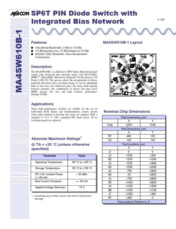
MA4SW510B-1 Layout
Ultra Broad Bandwidth: 2 GHz to 18 GHz 1.9 d B Insertion Loss, 35 d B Isolation at 18 GHz Reliable. Fully Monolithic, Glass Encapsulated Construction
Description
The MA4SW610B-1 is a Reflective SP6T Series-Shunt broad band switch with integrated bias networks made with M/A-’s HMICTM (Heterolithic Microwave Integrated Circuit) process, US Patent 5,268,310. This process allows the incorporation of silicon pedestals that form series and shunt diodes or vias by imbedding them in low loss, low dispersion glass. By using small spacing between elements, this bination of silicon and glass gives HMIC devices low loss and high isolation performance through 18 GHz.
Applications
These high performance switches are suitable for the use in multi-band ECM, Radar, and instrumentation control circuits where high isolation to insertion loss ratios are required. With a standard +5 V/-5 V, TTL controlled PIN diode driver, 80 ns switching speeds are achieved.
Nominal Chip Dimensions
Chip Dimensions (µm) X 3370 Pad Dimensions (µm) X 400 125 Y 3120 Y 125 125
Chip
Absolute Maximum Ratings1 @ TA = +25 °C (unless otherwise specified)
Parameter Operating Temperature Storage Temperature RF C.W. Incident Power (+/-20 m A) Bias Current (Forward) Applied Voltage (Reverse) Value -65 °C to +125 °C -65 °C to +150 °C + 30 d Bm +/- 40 m A 15 V
RF DC
1. Exceeding any of these values may result in permanent damage
J1 J2 B2 J3 B3 J4 B4 J5 B5 J6 B6 J7 B7
Pad Locations (µm) X Y 0 0 -1535 +300 -1535 +1000 -1535 +1800 -1535 +2500 -750 +2820 -50 +2820 +750 +2820 +1450 +2820 +1535 +1800 +1535 +1100 +1535 +300 +900 0 Pad Locations Relative to J1
SP6T PIN Diode Switch with Integrated Bias Network
V 1.00
Electrical Specifications @ TA = 25 °C, +/- 10 m A Bias Current (On-Wafer Measurements)
Parameters
Insertion Loss
Frequency
6 GHz 12 GHz 18 GHz
Minimum
43 35 30
- Typical
1.0 1.3 1.9 49 43 39 18 20 16 19 22 20 80
Maximum
1.4 2.0 2.9
-...