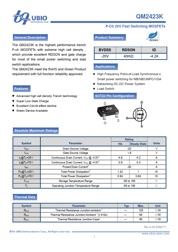
GENERAL DESCRIPTION
FEATURES
z Advanced high cell density Trench technology z Super Low Gate Charge z Excellent Cdv/dt effect decline z Green Device Available Product Summery BVDSS -20V RDSON 40mΩ ID -4.2A APPLICATIONS
z High Frequency Point-of-Load Synchronous s Small power switching for MB/NB/UMPC/VGA z Networking DC-DC Power System z Load Switch SOT23 Pin Configuration D ABSOLUTE MAXIMUM RATINGS
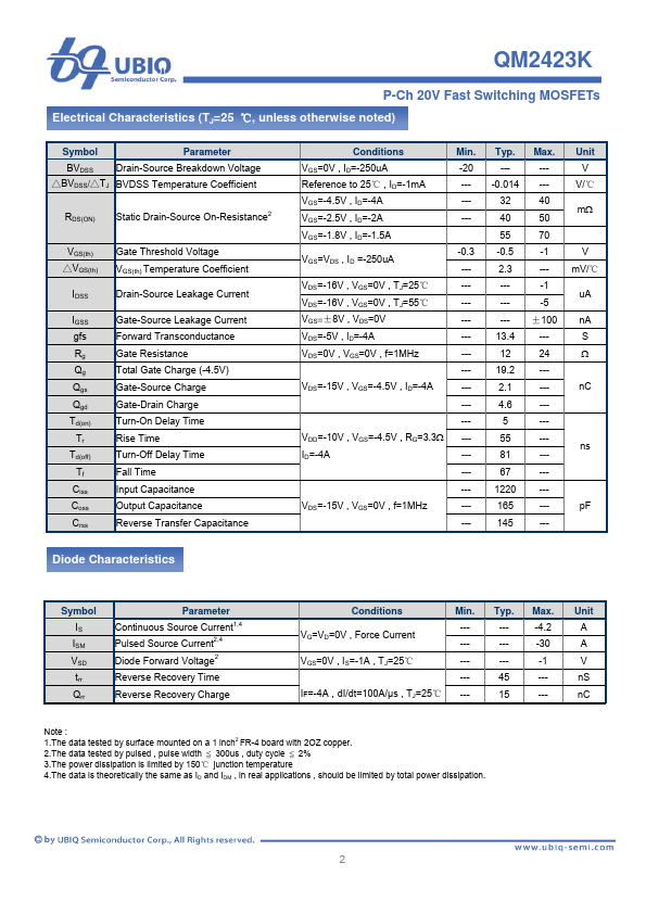
G Symbol VDS VGS ID@TA=25℃ ID@TA=70℃ IDM PD@TA=25℃ PD@TA=70℃ TSTG TJ Parameter Drain-Source Voltage Gate-Source Voltage Continuous Drain Current, VGS @ -4.5V1 Continuous Drain Current, VGS @ -4.5V1 Pulsed Drain Current2 Total Power Dissipation3 Total Power Dissipation3 Storage Temperature Range Operating Junction Temperature Range S Rating 10s Steady State -20 ±8 -4.8 -4.2 -3.9 -3.4 -30 1.32 1 0.84 0.64 -55 to 150 -55 to 150 Units V V A A A W W ℃ ℃ Thermal Data Symbol RθJA RθJA RθJC Parameter Thermal Resistance Junction-ambient 1 Thermal Resistance Junction-Ambient 1 (t ≤10s) Thermal Resistance Junction-Case1 1 Typ. ------- Max. UBIQ