AOSP21321 Overview
Key Specifications
Max Operating Temp: 150 °C
Min Operating Temp: -55 °C
Description
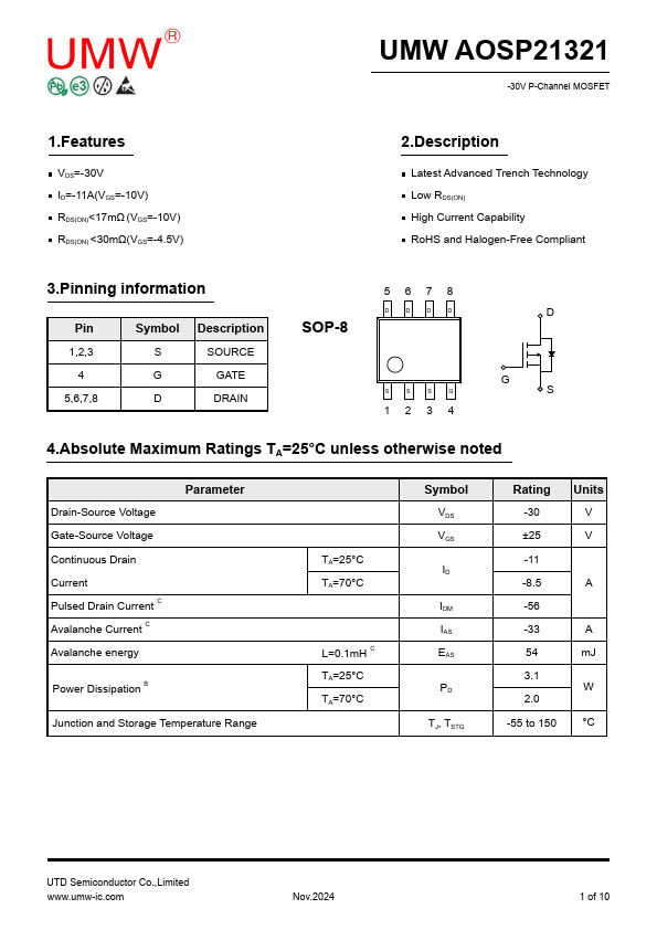
SOURCE GATE DRAIN SOP-8 5678 D D D D S S S G 1234 D G S Drain-Source Voltage Gate-Source Voltage Continuous Drain Current Pulsed Drain Current C Avalanche Current C Avalanche energy Parameter Power Dissipation B Junction and Storage Temperature Range TA=25°C TA=70°C L=0.1mH C TA=25°C TA=70°C Symbol VDS VGS ID IDM IAS EAS PD TJ, TSTG Rating -30 ±25 -11 -8.5 -56 -33 54 3.1 2.0 -55 to 150 Units V V A A mJ W °C UTD Semiconductor Co.,Limited Nov.2024 1 of 10 UMW AOSP21321 -30V P-ChanneI MOSFET Characteristics Parameter Symbol Typ Max Units Maximum Junction-to-Ambient A t ≤ 10s RθJA Maximum Junction-to-Ambient A D Steady-State 31 40 °C/W 59 75 °C/W Maximum Junction-to-Lead Steady-State RθJL 16 24 °C/W 2 of 10 UTD Semiconductor Co.,Limited Nov.2024 UMW AOSP21321 -30V P-ChanneI MOSFET Characteristics (TJ=25°C unless otherwise noted) Parameter STATIC PARAMETERS Drain-Source Breakdown Voltage Zero Gate Voltage Drain Current Gate-Body leakage current Gate Threshold Voltage Static Drain-Source On-Resistance Forward Transconductance Diode Forward Voltage Maximum Body-Diode Continuous Current DYNAMIC PARAMETERS Input Capacitance Output Capacitance Reverse Transfer Capacitance Gate resistance SWITCHING PARAMETERS Total Gate Charge Total Gate Charge Gate Source Charge Gate Drain Charge Symbol Conditions Min Typ Max Units BVDSS ID=-250µA, VGS=0V -30 V VDS=-30V, VGS=0V IDSS TJ=55°C -1 µA -5 advanced VDS=0V, VGS=±25V ±100 nA VGS(th) VDS=VGS, ID=-250μA -1.3 -1.8 -2.3 V V.