Datasheet4U.com
🌙
P0610BT Datasheet | UNIKC
Part:
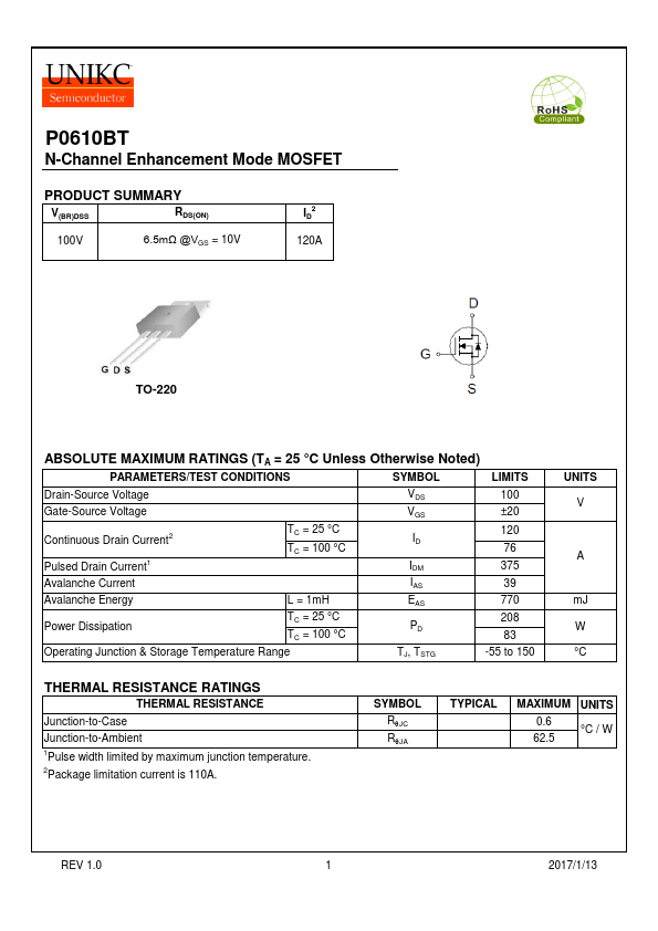
P0610BT
Description:
N-Channel MOSFET
Category:
MOSFET
Manufacturer:
UNIKC
Size:
710.06 KB
P0610BT Datasheet (PDF) Download
Related P0610BT Datasheets
P0610BTF N-Channel MOSFET
UNIKC
P0610BT
Datasheets by Manufacturer
Part Number
Manufacturer
Description
P0610BTF
NIKO-SEM
N-Channel Transistor
×
Close