The following content is an automatically extracted verbatim text
from the original manufacturer datasheet and is provided for reference purposes only.
View original datasheet text
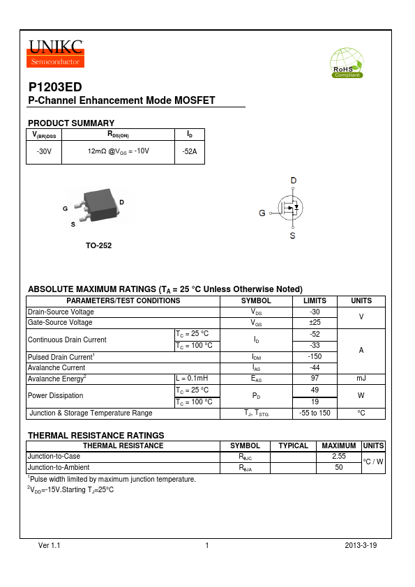
P1203ED
P-Channel Enhancement Mode MOSFET
PRODUCT SUMMARY
V(BR)DSS
RDS(ON)
-30V
12mΩ @VGS = -10V
ID -52A
TO-252
ABSOLUTE MAXIMUM RATINGS (TA = 25 °C Unless Otherwise Noted)
PARAMETERS/TEST CONDITIONS
SYMBOL
LIMITS
Drain-Source Voltage
VDS -30
Gate-Source Voltage
VGS ±25
Continuous Drain Current Pulsed Drain Current1
TC = 25 °C TC = 100 °C
ID IDM
-52 -33 -150
Avalanche Current Avalanche Energy2
L = 0.1mH
IAS EAS
-44 97
Power Dissipation
TC = 25 °C TC = 100 °C
PD
49 19
Junction & Storage Temperature Range
TJ, TSTG
-55 to 150
UNITS V
A
mJ W °C
THERMAL RESISTANCE RATINGS
THERMAL RESISTANCE Junction-to-Case
Junction-to-Ambient 1Pulse width limited by maximum junction temperature. 2VDD=-15V.Starting TJ=25°C
SYMBOL RqJC RqJA
TYPICAL
MAXIMUM 2.