The following content is an automatically extracted verbatim text
from the original manufacturer datasheet and is provided for reference purposes only.
View original datasheet text
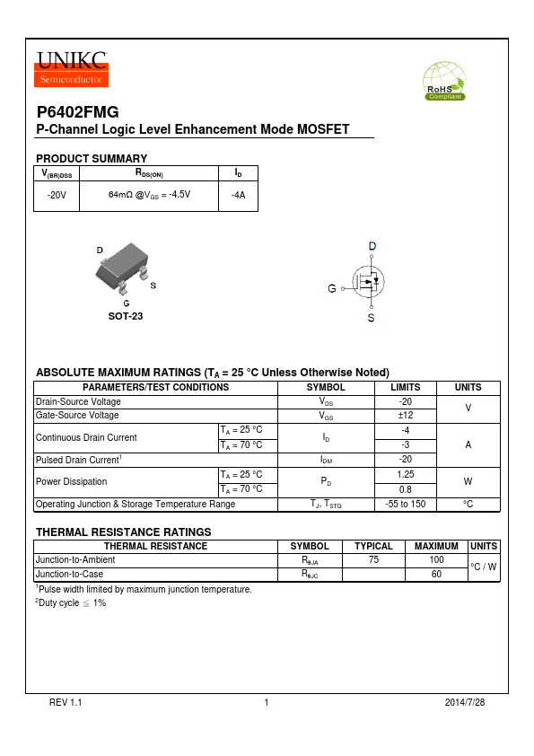
P6402FMG
P-Channel Logic Level Enhancement Mode MOSFET
PRODUCT SUMMARY
V(BR)DSS
RDS(ON)
-20V
64mΩ @VGS = -4.5V
ID -4A
SOT-23
ABSOLUTE MAXIMUM RATINGS (TA = 25 °C Unless Otherwise Noted)
PARAMETERS/TEST CONDITIONS
SYMBOL
LIMITS
Drain-Source Voltage
VDS -20
Gate-Source Voltage
VGS ±12
Continuous Drain Current Pulsed Drain Current1
TA = 25 °C TA = 70 °C
ID IDM
-4 -3 -20
Power Dissipation
TA = 25 °C TA = 70 °C
PD
1.25 0.8
Operating Junction & Storage Temperature Range
TJ, TSTG
-55 to 150
UNITS V
A
W °C
THERMAL RESISTANCE RATINGS
THERMAL RESISTANCE Junction-to-Ambient Junction-to-Case 1Pulse width limited by maximum junction temperature. 2Duty cycle ≦ 1%
SYMBOL RqJA RqJC
TYPICAL 75
MAXIMUM 100 60
UNITS °C / W
REV 1.